


EMC: A mapping for the Compact Muon Solenoid CMS experiment
Fernando José González Arteche
TESIS DOCTORAL UNIVERSIDAD DE OVIEDO
Departamento de Ingeniería Eléctrica, Electrónica, de Computadores
y Sistemas
ABSTRACT
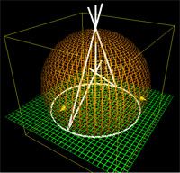
Introduction The Compact Muon Solenoid (CMS) is one of the four high-energy physics experiments under construction at CERN for the Large Hadron Collider (LHC) accelerator. The dimensions of the CMS detector are about 30 meters long and 25-meter diameter, with a total weight of around 13000 tons. The CMS detector is divided in five sub-systems located at different layers of the structure. Each sub-system has distinct objectives and processes different signal and energy levels. In general, high-energy physics (HEP) experiments identify particle interactions and measure their energy using sensitive detection devices such as silicon and pixel detectors, wire chambers, scintillators and optical devices. In the CMS experiment, the detected electrical signal is amplified and processed by the front-end electronics (FEE), which communicate, via optical links, with the acquisition system located 120 meters away from the detector. The read-out electronics of the CMS experiment are designed to process signals of a few mV digitizing them synchronously at 40 MHz. Part of this electronics is located inside of a harsh environment with particle radiation and a DC magnetic field of 4 Tesla.
FULL THESIS
https://copy.com/jpKjlUr08vtbguho


 JOSIL ARTISTA PLASTICO FORTALEZA CEARA BRASIL AV.HERACLITO GRAÇA 41 TEL(85)32542378


Nenhum comentário:
Postar um comentário