domingo, 10 de janeiro de 2010
GE estuda criação de centro de pesquisas e desenvolvimento no Brasil
Em comunciado da GE, o presidente e Chief Executive Officer (CEO) global da companhia, Jeff Immelt, diz que "o Brasil é a escolha lógica para a instalação?. Na avaliação do executivo, um laboratório de pesquisa industrial ajudará a companhia a formar parcerias mais fortes com nossos clientes.
quinta-feira, 7 de janeiro de 2010
Optimization of Powder Core Inductors of Buck-Boost Converters for Hybrid Electric Vehicles


Suwon, Korea
Gwang-Bo Choi
R&D Center
Changsung Corporation
Incheon, Korea
JNEX-Core®, amorphous and ferrite cores are compared for the
inductor of buck-boost converter for Hybrid Electric Vehicles
(HEVs). The core losses are analyzed at the condition of 10kHz
sine wave excitations. Permeability fluctuations vs. temperature
and magnetizing force will be analyzed and discussed. Under the
specifications of buck-boost converter for 20kW THS-II, the
power inductor will be designed with Mega-Flux®, JNEX-Core®
and the informative simulation results will be provided with
respect of dc bias characteristics, core and copper losses.
Keywords- HEVs; Buck-Boost Inductor; High power density;
Low core loss; Thermal stability; Leakage flux
ESTE ARTICULO COMPLETO LO ENCUENTRAS EN MI WEBSITE:http://caveromiranda.galeon.com/
sábado, 2 de janeiro de 2010
IGBT Behavior under Short and Fault Protection
In inverter driven UPS or motor applications, the IGBT can be destroyed when it is
turned-on into a faulted motor or an output short circuit or an input bus voltage shoot
through. Under these conditions current through the IGBT increases rapidly until it
saturates. After fault detection, depending on the point at which the fast turn-off pulse is
applied, very different levels of hole current can flow under the n+ source region, making
this an important factor in the successful containment of the fault current. We present
experimental observations showing that IGBT failure under short-circuit conditions is
dependent on where and how the turn-off pulse is applied. A two-step (two-level) turn-off
gate driver circuit is introduced which safely turns-off even a high transconductance
IGBT during short-circuit and abnormal over current faults. This turn-off process starts
during faulted condition only.
By Sampat Shekhawat and Bob Brockway, Fairchild Semiconductor.
It is very common that an IGBT used for motor drive, UPS and some
other industrial applications, be selected for 10 micro-second shortcircuit
withstand time (SCWT) if regular de-sat protection driver is
used. But this driver generates high turn-off stress to the IGBT during
inverter short circuit or the output becomes faulty. Under these abnormal
conditions when the IGBT is turned-off abruptly, failures can
occur if the IGBT is not selected properly. If the smart fault protection
is not used, high turn-off loss will be generated and even short circuit
current can ramp-up to a dangerous level destroying the IGBT. There
are several ways to turn-off the IGBT once fault condition is detected.
Some of these are as follows:
Gate is discharged through high gate resistance. This discharge path
is activated only during the above said abnormal conditions. This is
not the best solution.
Gate voltage is abruptly reduced to zero.
Adding some source inductance which is common for both gate discharge
path and load current.Gate de-bias occurs. But during normal
condition switching loss is increased.
Sense IGBT can also be used where fault current is sensed by pilot
cell but the current sense accuracy of these pilot cells is not good
which is further is affected by temperature.
Gate voltage pattern analyzer for short-circuit protection in IGBT
inverters [1]. These circuits are very sensitive to load changes and
type of loads.
Current sense resistor or Hall-effect devices are also used to detect
fault through IGBT. But again these methods either generate power
loss or are costly.
But de-sat protection is the most commonly used for short-circuit and
over current fault protection. De-sat detection truly provides the state
of electrical over stress of IGBT under current fault condition when
gate voltage is high. Reducing gate voltage in a controlled manner to
just above gate threshold voltage is preferred and described in this
article. This will reduce fault current and after some finite time gate
voltage is brought down to zero safely, turning-off the IGBT without
stress.
Gate Drive Circuit
The main function of any gate driver circuit is to convert a control signal
to a power signal that can efficiently controls the IGBT or MOSFET
turn-on and turn-off. If the IGBT or MOSFET requires short circuit
protection, the gate drive circuit must safely turn-off the switch
during a shorted or abnormal overload condition. A more detailed list
of the gate drive circuit requirements for an IGBT or MOSFET are as
follows:
A controlled turn-on and turn-off of the IGBT so as to optimize the
conduction and switching losses.
In some applications, electrical isolation between control circuit and
power circuit is very important.
In the case of a short circuit condition, the IGBT should be protected
and turned-off safely with minimum power dissipation and stress. The
gate drive circuit should be able to minimize short circuit current and
short-circuit withstand time without device failure. If both of these
parameters are minimized, the power dissipation under short circuit
will reduce and the system reliability will increase.
During a short circuit condition, the IGBT collector to emitter voltage
can rise fast. The voltage across the gate to emitter should not be
allowed to rise due to gate to collector displacement current flowing
into the gate to emitter capacitance, Cge. Current flowing into Cge
will cause Vge to rise and further increase the short circuit current.
One should make sure that this condition is avoided.
Preferably a totem pole output stage with separate turn-on and turnoff
resistance option. The gate discharging switch of the totem pole
should be as close as possible to IGBT and minimize the loop inductance
between this switch and IGBT gate & emitter terminals.
Minimize the propagation delay time between input and output pulses
of the gate driver.
De-Saturation
The de-saturation detection technique for identifying a short circuit
and fault condition in an IGBT is well known. Generally, a de-saturation
condition is said to exist if the voltage across the IGBT collector
to emitter terminals rises above 5-8 volts while the gate to emitter
voltage is high. This condition indicates that the current through the
IGBT has exceeded the normal operating level. The gate drive circuit
should be designed so that it reacts promptly to the short circuit and
safely turns-off the IGBT within SCWT rating of the IGBT. However, in
recent years, IGBTs have been designed with lower conduction and
switching losses but this generally reduces SCWT. IGBT technology
utilizes shallow junctions to decrease switching and conduction losses.
However these new technologies have increased the transconductance
(gm) of the IGBT. Since the magnitude of the IGBT short
circuit current is directly proportional to gm, during a short-circuit condition,
a higher collector current results. The large collector current
and high bus voltage place the IGBT in a state of high instantaneous
power dissipation that can only be sustained for a few microseconds.
The gate drive circuit must respond very quickly and efficiently to the
fault current to protect the IGBT. Due to the two-step turn-off, the
IGBT with even 4 microseconds short circuit withstand time can safely
be turned-off and protected. The IGBT, used in conjunction with the
two-step turn-off gate drive, safely turns off low impedance over-current
faults and shorted bus conditions where single-step gate drivers
fail. The Industry standard (10 μs) SCWT is no longer required when
the IGBT is used with this gate driver.
IGBT Behavior during short circuit and over current
The peak current during a short circuit is limited by the gm of the
IGBT. Moreover, the rate of rise of the current is limited by the turnon
characteristics of the IGBT in combination with common emitter
inductance. If IGBT collector current does not saturate and reach a
state of equilibrium and bus voltage has not raised high enough
attempting to turn off the IGBT during can lead to IGBT latch-up [2].
In case of fault conditions very different hole current flow under n+
source regions. These different hole current conditions and patterns
of hole current under n+ source generate different electrical stress. In
case if the gate voltage is brought down abruptly to zero before
device voltage reaches clamp, the IGBT can latch-up and fail. Flow
of electron through the channel is cutoff once the gate is turned off.
Holes continue to inject from emitter of p-n-p structure which is
known as IGBT collector. This process stops when electrons in IGBT
N-base are depleted. At this point IGBT current is almost all hole current.
The amount of holes is very high here and if IGBT does not
reach clamp voltage IGBT can latch-up and fail. However if enough
time is allowed to complete this process and plasma of electrons in
IGBT N-base is reduced or depleted so that base current reaches
zero. At this point the carriers from emitter of IGBT p-n-p transistor
are no longer injected and IGBT current is almost all hole current.
IGBT voltage rises at a rate so that edge of the depletion spread can
sweep out enough carriers to maintain inductive current. If enough
time is allowed to stabilize the bus voltage while the channel current
is flowing, the IGBT N-base is depleted and because of this current
flow is more uniformly distributed. The displacement current becomes
very small since dv/dt reduces and latch-up is avoided. If enough
time is not allowed for the IGBT to reach clamp voltage and gate voltage
is removed abruptly, IGBT voltage will rise with high dv/dt and
current in IGBT is non-uniformly distributed, high displacement current
generated by high dv/dt can latch-up IGBT. Non-uniform gate
ESR combined with Miller capacitance result in non-uniform turn-off
of IGBT active area. This results into high localized hole current density
flowing laterally in P-base of parasitic n-p-n bipolar resulting in
latch-up of parasitic thyristor. Because of these reasons one has to
wait untill IGBT reaches clamp voltage collector current saturates. So
it is safer to choose IGBT with 10 microseconds SCWT for motor
drive and UPS inverter applications if a regular gate driver is used.
Two step soft turn-off gate drive
It is clear that if the collector to emitter voltage rises to the DC Bus
slowly and high transconductance increases short circuit current, regular
driver does not protect an IGBT with a low short circuit withstand
time (<5us). However the longer SCWT comes at the cost of higher
switching and conduction losses. The rate of rise of the collector to
emitter voltage is dependent upon the operating conditions and can
take several microseconds to rise to bus voltage. However, the gate
drive must respond quickly to initiate turn off to protect a low SCWT
IGBT. The only solution is to lower the gate voltage to just above
threshold voltage of the IGBT. The IGBT reaches clamp voltage
faster and reduces IGBT current during fault.
Power Module Reliability-Confiabilidad Modulos de Potencia
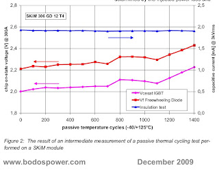
The reliability of a power module is of vital importance to the user, who expects his
system to work unimpaired throughout its entire service life. The elimination of the base
plate offers clear design engineering advantages that boost system reliability. In fact,
modules without a base plate can be expected to have an extended service life especially
with respect to stress induced by passive thermal cycles.
By Dr. Uwe Scheuermann, Manager Product Reliability, SEMIKRON.
Conventional power modules feature solid copper base plates. This design concept brings about a number of disadvantages with regard to reliability. In most cases, the base plates are joined to the heat sink by way of screw connections at the corners or, in the case of larger modules, along the outer edges. In these cases, to ensure optimum heat transfer between base plate and heat
sink in the centre region as well, the base plate has to be suitably deflected before mounting.
The stress resulting from the different coefficients of thermal expansion of the base plate and substrate does not, however, only play a key role in manufacturing but also when the system is in operation. In application, a power module is exposed to significant temperature fluctuations. On the one hand, these thermal cycles are caused by the power loss produced in the power electronic component. These active thermal cycles are determined by the injected power loss and the thermal resistance of the module. Generally speaking, it is possible to reduce the
temperature swing by enlarging the siliconarea of the components, thus reducing the
thermal resistance.
In the case of passive thermal cycles, byway of contrast, this is not possible. Passive
cycles result from ambient temperature changes. For a power module, such stresses
are caused by a temperature change in the heat sink which in turn may result from a
change in the coolant temperature or from power losses in other components. The load
cycling capability in the case of passive temperature swings is determined by the module design alone; it cannot be enhanced by increasing the silicon area.
POWER MODULOS Pressing Home the Advantages


Pressing Home the Advantages
Press-Fit pin for solder-less assembly
Solder pins have been the interface of choice for power modules for many years. The new
press-fit pin developed by Vincotech takes the assembly properties of Vincotech power
modules a step further: the solder-less assembly of the modules, equally easy on both
sides of the PCB, leads to higher reliability and design flexibility and drastically reduces
production costs.
By Peter Sontheimer, Vincotech
The target: faster and easier assembly
Common inverter construction today features large Through The Hole
(TTH) components along with smaller SMD devices on one side of
the PCB, with the power module mounted on the other side and connected
to the heat sink (see fig 1). Only in exceptional cases, where
space allows and where special heat sink shapes are possible, the
power module is mounted on the same side as all other components.
This means that wave-soldering of the power module is not possible.
The solution most usually adopted in these cases is either a manual
solder process, which immediately raises questions regarding reliability
and production efficiency, or selective robot soldering, entailing the
same production efficiency issues as well as higher costs.
Simulation software to calculate heatsink.

SemiSimV1 is a Powerful simulation and calculation program for power electronics.
The simulation program consists of the following modules:
Mod1: power loss calculation for buck and boost converters, 3-phase inverters and Indirect Matrix Converter.
Customer-specific adaptations are possible.
Mod2: temperature of the silicon and lifetime calculations for defined load cycles
Mod3: Thermal resistance and thermal conductivity of VIA's and PCBs in different lay-out
Mod4: Heatsink calculation, heat resistance and heat transfer coefficient calculation of heat sinks in natural convection and active.
Mod5: 2-D simulation of heat sink temperature in accordance with the heat spreading and thermal conductivity of heat sink.
Heat sink temperature calculated
Database for the collection of IGBT, MOSFET, diode and thyristor data
Be determined for a long life and reliable operation of power electronics, the semiconductor temperature. In many cases, a heat sink is used for cooling. Be known for the determination of the semiconductor temperature, the temperature of the heatsink.
The heat sources are usually not distributed homogeneously on the heatsink. Thus, the heat distribution as a function of the position of the heat sources can be simulated.
There are excellent simulation programs to perform the calculation based on the finite element method. This is often drawn a 3-Dimensional Model of the heat sink. The model is divided into a corresponding number of elements. The result deserting method is very accurate.
The disadvantage is the high complexity and high cost of such programs.
Another important point is the correct value for the thermal resistance (heat resistance) of the heatsink. This value is dependent on the geometry, imprinted on the type of cooling or dissipation of the heat sink is. This value is not found in the data sheets of manufacturers, as it depends on the previously described parameters.
SemiSimV1 the Modul4 and Modul5 is a very inexpensive program that allows a first estimation of the temperature distribution and heat sink temperature. The required thermal resistance of heat sink can be calculated quickly and easily.
The program does not provide the exact dates of a "Finite Element Simulation", however, allows the developer from the beginning of the heat sink to calculate and simulate the temperature of the heat sink.
Thermal Analysis of Semiconductors


and life time of semiconductors.
The design of power converter includes necessarily the calculation of power loss and
temperature rise in the semiconductors and heat sink. This article shows the procedure of
evaluation junction temperature and life time of semiconductors.
By Tobias Hofer, Negal Engineering GmbH Switzerland.
The design of power converter includes necessarily the calculation of
power loss and temperature rise in the semiconductors and heat
sink. For a reliable design the temperature ripple of the silicon should
also be considered. The temperature ripple mainly determines the life
time of the semiconductor (number of cycles to failure). The junction
temperature is related to the heat sink temperature. Mostly the heat
sources are not homogenous distributed over the heat sink. Therefore,
the heat distribution on the heat sink must be known.
Case temperature
The lifetime of the power module not only depends on the temperature
difference ΔTj but also on the average junction temperature of
the semiconductor. It makes a difference whether the temperature
swing of 30K is between 60°C and 90°C or between 80°C and
110°C. It takes a much smaller number of cycles to failure if the
absolute temperature is higher. The junction temperature is relative to
the case temperature of the semiconductor module. The fact that the
heat sources (semiconductors) are not evenly spread over the heat
sink, the heat distribution of the heat sink must be simulated. The
simulation tool used for the simulation in this paper represents the
heat sink as a rectangular plate. One side is cooled by convection.
On the other side rectangular heat sources are placed. The top of the
heat sources and heat sink is isothermal.
For a reliable design of the power converter it is important to calculate
the semiconductors temperature. The significance of simulating
the temperature distribution on the heat sink was shown. Taking the
temperature ripple and the average temperature of the semiconductor
in account leads to safer designs. With adequate simulation software
it is possible to optimize the design during the development
process in an early stage. All simulations in this paper were performed
with SemiSimV1 [3].
References
[1] Realistic benchmarking of IGBT-modules with the help of fast and
easy to use simulation-tool
R.Schnell, U.Schlapbach; ABB Switzerland
[2] Power Cycling Lifetime of Advanced Power Modules for Different
Temperature Swings U.Scheuermann, U.Hecht; SEMIKRON
[3] SemisSimV1, www.negal.ch
sexta-feira, 1 de janeiro de 2010
ENTREVISTA AL MATEMATICO PERUANO PROF. SR. CESAR CAMACHO
El día sábado 6 de septiembre se publicó, en el diario El Comercio, una entrevista realizada al matemático César Camacho. El tema de la entrevista versó sobre la ciencia en el Perú, específicamente la matemática. El doctor Camacho, con la gran trayectoria ganada en todo el mundo, nos presenta su visión acerca de la fuga de cerebros que viene padeciendo nuestro país. En este blog ya comentamos un poco de esta problemática. Asimismo, acerca de la vida de este gran matemático que ahora labora en el IMPA.
Les anexo la entrevista y espero dejen sus comentarios.
“El Perú exporta talento y eso es una insensatez, un absurdo”
El matemático más importante del Perú afirma que mil científicos peruanos de nivel de excelencia aportan al desarrollo de otros países. Es necesario una clara política de Estado
LA FICHA
Nombre: César Leopoldo Camacho Manco.Nació: Barranco, abril de 1943.Estudios: GUE Alfonso Ugarte. Ingeniería de minas y matemática pura en la UNI. Doctorado en matemática en la Universidad de Berkeley.Trayectoria: Director del Instituto Nacional de Matemática Pura (IMPA) de Brasil. Tiene 40 trabajos y 9 libros publicados. La PUCP le otorgó en el 2006 el Premio Southern Perú y la medalla Cristóbal de Lozada y Puga a la creatividad humana. Mundialmente se le reconoce la solución a un problema clásico propuesto en el año 1856 y que hoy se conoce como teorema de la separatriz de Camacho-Sad.
Fuente: El Comercio









 JOSIL ARTISTA PLASTICO FORTALEZA CEARA BRASIL AV.HERACLITO GRAÇA 41 TEL(85)32542378