AUTOR DO BLOG ENG.ARMANDO CAVERO MIRANDA SÃO PAULO BRASIL

"OBRIGADO DEUS PELA VIDA,PELA MINHA FAMILIA,PELO TRABALHO,PELO PÃO DE CADA DIA,PROTEGENOS DO MAL"

"OBRIGADO DEUS PELA VIDA,PELA MINHA FAMILIA,PELO TRABALHO,PELO PÃO DE CADA DIA,PROTEGENOS  DO MAL"

“SE SEUS PROJETOS FOREM PARA UM ANO,SEMEIE O GRÂO.SE FOREM PARA DEZ ANOS,PLANTE UMA ÁRVORE.SE FOREM PARA CEM ANOS,EDUQUE O POVO.”

“Sixty years ago I knew everything; now I know nothing; education is a progressive discovery of our own ignorance. Will Durant”

segunda-feira, 29 de maio de 2017

A Practical Study on Three-Level Hybrid SiC/Si Inverters Fabio Brucchi at Infineon Technologies Italia S.r.l. Klaus Sobe and Davide Chiola at Infineon Technologies Austria AG


In today’s PV, UPS and GPI systems, three-phase output inverters are often based on three-level topologies using Silicon IGBTs. This article demonstrates the potential of a hybrid inverter using CoolSiCTM MOSFETs and TRENCHSTOPTM 5 Silicon IGBTs.
State of the Art Three-Level Inverter Topologies Three-level inverters based on Silicon IGBTs are a common design solution giving an excellent cost/performance ratio. As explained in [1]-[3], the technical advantage over the classical two-level B6 inverter represented in Figure 1 (a) is a reduction of switching losses and filtering effort, at the expenses of higher circuit complexity. Two commonly found three-level designs in the low to mid power range are the Neutral Point Clamping Diode and the Neutral Point Clamping Transistor topology, illustrated in figure 1 (b) and (c), respectively.

Figure 1: Commonly used inverter configurations: (a) two-level (B6, Six-Pack) inverter; (b) three-level neutral point clamping diodes (NPC-1, I-Type) inverter; (c) three-level transistor clamped (NPC-2, T-Type) inverter; for each topology only one out of three phases is shown.
As explained in [2], [4] and [5], both three-level topologies have their advantages and disadvantages. While T-Type inverters have fewer semiconductor devices on the current path and thus low conduction losses, I-Type inverters benefit from lower switching losses as there is no need for a relatively slow higher voltage device. Consequently, T-Type inverters are typically found at switching frequencies up to 20-30kHz, I-Type inverters above.

 SiC Technology Changes the Picture

The unique features of Silicon Carbide (SiC) switches were described in [7] and [8] together with the potential impact on applications. With the emerging SiC semiconductor technology the degrees of freedom for the designer become higher, opening the path to new scenarios: fast 1200V SiC switches can make T-Type inverters attractive for higher frequencies and even the transition back to a two-level solution might be considered in order to achieve higher efficiency and reduce the bill of material [6]. In the following sections, the potential of a hybrid T-Type inverter using 1200V CoolSiC™ MOSFETs and 650V TRENCHSTOPTM 5 IGBTs is demonstrated experimentally. The key benefits of this approach are low conduction and switching losses, relatively low effort for output and EMI filtering and – compared to converters with more than three levels – moderate control effort. 
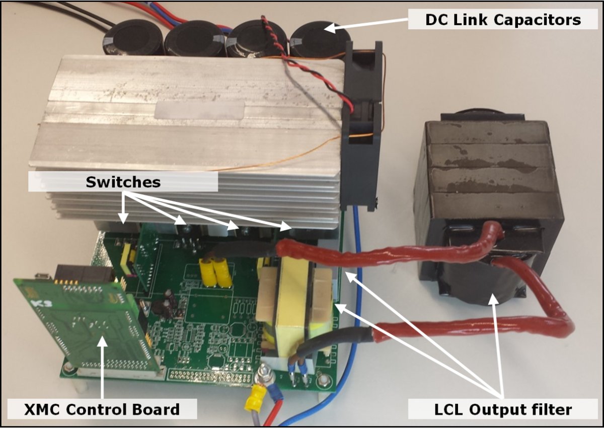
Test Setup and Conditions Since this article considers the influence of only the power semiconductors on the system efficiency, all measurements were carried out using a single phase test board and a fixed L-C-L output filter designed by Tecnologie Future S.r.l. and Infineon Technologies Austria A.G. The design goals for this platform were a simple component replacement as well as an easy access for thermal and electrical measurements – not a demonstration of power density or a BOM cost reduction. It should be noted that the absolute efficiency values obtained with a single-phase system do not correspond one-to-one to the values of a three-phase and three-wire system, i.e. a system without exposed neutral. First, the core losses of the filters are different and second the modulation scheme cannot use a third-harmonic injection technique. All devices were operated using an Infineon 1EDI60N12AF driver. This compact, isolated, single channel driver is based on the coreless transformer technology, featuring a high common mode transient immunity – a major requirement when dealing with high speed switches. The output voltage of the drivers is provided using a local HF transformer close to the driver that is fed from one resonant AC link. Using the turn-ratio of the transformer, the gate voltages are set to +15V for turn-on and -5V for turn-off. The single phase inverter was operated at a constant DC link voltage of 720VDC providing a voltage of 230VRMS on the output. Using an electric AC load the output current of the inverter was increased in steps of 1,5ARMS every 5 minutes in order to determine the conversion efficiency for different load situations.
 LINK ORIGINAL
https://eepower.com/power-converters/practical-study-three-level-hybrid-sicsi-inverters-infineon-877#disqus_thread

sábado, 27 de maio de 2017

A Study on the Failure Mode of the Battery for Energy Storage System Kim Hee-Jung Department of Mechanical Design Engineering Pusan National University


Abstract
 Entering the 21st century, new & renewable energy, electric vehicle (EV) and energy storage system (ESS) have emerged due to more regulations on CO2 gases and depletion of fossil fuels after climate changes. With a leap towards the 'IT Era,' uninterruptible power supply (UPS) has developed into an essential equipment, an emergency power system designed to prevent a blackout. A key element of these facilities is a secondary battery which can be divided into lead-acid battery, Ni-MH, Ni-Cd and lithium ion battery (LIB). In particular, there have been numerous studies on lithium batteries with the following advantages: i) low price for unit volume and energy density by weight, ii) very stable lead-acid and high energy density, iii) long life expectancy. The valve-regulated lead-acid battery (VRLA) designed for power storage has a long life expectancy that is 3,000 times or more at 70% depth of discharge. Since it is a closed type, it can suppress the decrease of the electrolyte level, making maintenance unnecessary. In this kind of the VRLA designed for power storage (e.g. photovoltaic power generation, wind power generation, load leveling, etc.), battery performance and life are dependent upon lead alloy-based grid casting and electrolyte 'gel' mixing technologies. Regarding energy accumulation for optimum system operation, the technology developed to figure out the progress of battery failure is a key factor. The conventional large stationary lead-acid battery is mostly used as a backup against a blackout. Even though its life expectancy increased to 15 years, it is not appropriate for power storage in which charge and discharge are repeated every day. These lead storage batteries have critical effects on battery life and performances depending on their charging system. Therefore, the design of an optimum charge system is crucial for operating an optimum system. In general, the suitability of an optimum charge system is assessed by measuring the degree of battery aging. Hence, this study attempted to derive the optimum charge system setting after assessing the degree of battery aging under diverse load conditions. According to high-temperature accelerated life testing, battery internal resistance almost doubled compared to the early-stage battery when the rated capacity decreased to 80% or less. At the same time, battery surface temperature increased by almost twice as well. The VRLA/GEL was primarily heated in the middle area. It appeared that a gel electrolyte was dried out because of heating, causing increase in temperature. In LIB, diverse cathode materials have been applied since the lithium ion secondary battery comprised of LiCOO2 was first developed by SONY. However, LiFePO4 and ternary battery are currently used most widely. LiFePO4 is 3.2V in operating voltage and 170mAh/g in theory capacity. Even though it is slightly lower than a ternary battery in terms of energy density, it has a low risk of ignition and explosion. Therefore, it is great in terms of battery safety. With the aforementioned properties, a lithium ion battery is advantageous in industrial battery sectors such as x-EV, ESS and UPS. Even so, LiFePO4 reveals very low electric conductivity as an olivine material (LiMPO4, M=Mn, Ni, Co, Fe). This weakness has been greatly improved by coating the surface of the active material with carbon. However, degradation becomes more severe because of increase in battery internal resistance as a cycle proceeds. The objective of this dissertation was to clarify failure mode of the secondary battery for ESS. Therefore, this study located the source of the heat which occurs at battery charge or discharge, using IR SnapShot Model 525, one of the non-destructive testing (NDT) and analyzed the progress of the degradation. Next, the degradation behavior and durability of lead storage battery were compared through the measurement of battery internal resistance. It was found that battery internal resistance almost doubled compared to the early-stage battery when the rated capacity decreased to 80% or less. At the same time, battery surface temperature increased by almost twice as well. The surface temperature and internal resistance of the lithium battery almost doubled respectively because of problems in the manufacturing process and the materials themselves.

3kW Energy Storage System with Solar Cells for Grid Connection Hong, Seongjun Department of Energy and Power Conversion Engineering UNIVERSITY OF SCIENCE AND TECHNOLOGY 2015


Abstract 
 In the near future, energy storage will play a vital role to enhance the present changing technology. Energy storage with power generation becomes necessary when renewable energy sources are connected to the grid which consequently adjoins to the total energy in the system since utilities require more power when peak demand occurs. This paper describes the operational function of a 3 kW grid-connected residential Energy Storage System (ESS) which is connected with Photovoltaic (PV) at its input side. The system can perform bidirectional functions of charging from the grid and discharging to the grid when power demand becomes high and low respectively. It consists of PV module, Power Conditioning System (PCS) containing a bidirectional DC/DC Converter and bidirectional DC/AC inverter and a Lithium-ion battery pack. ESS Configuration, specifications, and control are described. The bidirectional DC/DC converter tracks the maximum power point (MPPT) and maintains the stability of PV array in case of power deficiency to fulfill the load requirements. The bidirectional DC/AC inverter has good voltage regulation properties like low total harmonic distortion (THD), low electromagnetic interference (EMI), faster response and anti-islanding characteristics. Experimental results satisfy the effectiveness of the proposed system.
Keywords : energy

quinta-feira, 25 de maio de 2017

EnerSolar -SÃO PAULO-Brasil –23 A 25 MAIO 2017


A EnerSolar + Brasil –23 A 25 MAIO 2017- Feira Internacional de Tecnologias para Energia Solar chega em sua 6ª edição apresentando as mais recentes tecnologias, produtos e serviços voltados para o setor de energias sustentáveis, renováveis e limpas. Organizada pela Cipa Fiera Milano, a feira acontece anualmente todo o mês de maio, juntamente com o ECOENERGY – Congresso de Tecnologias Limpas e Renováveis para a Geração de Energia, que em 2017, realizará a sua 7ª edição.
NA EMPRESA ALPHA POWER DISTRIBUIDOR DE BATERIAS SELADAS E BATERIAS ESTACIONARIAS CRESCENDO CADA DIA NO MERCADO BRASILEIRO.

quinta-feira, 27 de abril de 2017

INFINEON HIGH POWER SEMINARIO TECNICO -TCT-ARTIMAR- SÃO PAULO BRASIL


Eng.Tiago Gomez da Silva (SMS LEGRAND-BRASIL) Eng. Armando Cavero Miranda (PERU) e Eng.David Levett Power Electronics Engineer at Infineon INFINEON HIGH POWER SEMINARIO TECNICO -TCT-ARTIMAR-27 abril - SÃO PAULO BRASIL


INFINEON HIGH POWER SEMINARIO TECNICO -TCT-ARTIMAR-27 ABRIL 2017 SÃO PAULO BRASIL 
 Foi realizado com muito sucesso hoje em São Paulo, o primeiro seminário técnico da divisão IPC (Industrial Power Control) da Infineon no Brasil. A TCT Brasil foi um dos organizadores do evento, que contou com a participação de diversos engenheiros da industria nacional com foco e aplicação nas linhas de IGBT e transistores bipolares de potencia. As palestras foram ministradas por engenheiros Alemães localizados na planta de Warstein.
Infineon High Power – Seminário Técnico
Quem são os palestrantes?
Adam Kwiatkowski
Technical Marketing Manager - Medium Power Bipolars
David Levett
Power Electronics Design and Application Engineer at Infineon Technologies
Michael Stelte
Technical Marketing Manager – Bipolars, Medium Power Disc Devices and Solder Modules
Localização:
São Paulo Center - Av. Lineu de Paula Machado, 1088 / 1100 – Cdi ade Jardim – SP
(em frente às tribunas especiais do Jockey Club)

Opening
Aula 1: What’s new on Infineon IGBT modules?
Aula 2: What’s new on Infineon Diodes and Thyristors?
Intervalo
Aula 3: Paralleling power devices. Design rules to get power devices to share
Aula 4: Measuring and Benchmarking Diodes and Thyristors
Almoço
Aula 5: Gate driver design. Isolation, power supplies, protection and pcb layout
Aula 6: Three level converters. What are the options and advantages/disadvantages?
Intervalo
Aula 7: How to drive and protect thyristors?
Aula 8: How to design for thermal performance on diodes/thyristors stacks?

Término do evento

segunda-feira, 24 de abril de 2017

A STUDY ON NOVEL PULSE POWER SUPPLY FOR MAGNETRON -KAN HEE PARK - MASTER PROGRAM IN ELECTRICAL ENGINEERING KONKUK UNIVERSITY


A STUDY ON NOVEL PULSE POWER SUPPLY FOR MAGNETRON USING HVC EMBEDDED HIGH FREQUENCY TRANSFORMER BY KANG HE PARK MASTER PROGRAM IN ELECTRICAL ENGINEERING GRADUATE SCHOOL OF KONKUK UNIVERSITY 

 ABSTRACT 

 A conventional power supply for driving magnetron has a ferro-resonant transformer ,a high voltage capacitor (HVC) and a high voltage diode.And it provides magnetron with 4000 volts DC ,which is produced by step-up transformer and doubler action of the diode and capacitor.

Though this power supply is simple,transformer is bulky,heavy and has low-fficiency.To improve hese defects a high frquency inverter type power supply has been investigated and developed in recent years.

However .because of additional control circuit and switching devices,inverter type power supply is more expensive than conventional one.Therefore.it is necessary to reduce production cost by all means.


This paper describes a novel HVC embedded high frequency transformer ,which embedding high voltage capacitor in its secondary winding.
LINK
http://www.mediafire.com/file/czruhtxse6a1r0m/STUDY_NOVEL_PULSE_POWER_SUPPLY_FOR_MAGNETRON.pdf

sexta-feira, 14 de abril de 2017

Design, Development and Control of >13 kV Silicon-Carbide MOSFET based Solid State Transformer (SST) by Gangyao Wang- North Carolina State University


Design, Development and Control of >13 kV Silicon-Carbide MOSFET based Solid State Transformer (SST) by Gangyao Wang 
A dissertation submitted to the Graduate Faculty of North Carolina State University in partial fulfillment of the requirements for the Degree of Doctor of Philosophy 
Electrical Engineering Raleigh, North Carolina

WANG, GANGYAO. Design, Development and Control of >13 kV Silicon-Carbide MOSFET based Solid State Transformer (SST).

 ABSTRACT
Within the advent of the smart grid system, the solid state transformer (SST) will replace the traditional 60 Hz transformer formed by silicon steel core and copper windings and provides the interface between the high distribution voltage and low utility voltage. Other than the smaller size and less weight, SST also brings many more functionalities including voltage regulation, reactive power compensation, power management and renewable energy integration. The motivation of this research is to design a solid state transformer based on the wide band-gap Silicon Carbide (SiC) power MOSFETs and compare it with the silicon IGBT based SST. With wider band-gap and higher critical electrical field, the high voltage SiC power device has advantages over silicon power device for both conduction and switching. An extensive study and characterization of the SiC MOSFET was first carried out. It has been found that the MOSFET parasitic capacitors store significant amount of energy and the MOSFET turn on loss is high but turn off loss is virtually zero with small enough turn on gate resistor. A method for estimating the MOSFET parasitic capacitances has been proposed and explained in detail. A PLECS loss simulation model has been developed for the >13 kV SiC MOSFET which has been verified through a boost converter with the SiC MOSFET switches under 40 kHz for both soft switching and hard switching conditions separately. Widely used full bridge circuit has been chosen as the topology for the SST rectifier for its simple structure and bidirectional power transfer capability. Form three different SPWM modulation methods, the bipolar single frequency SPWM method has been identified as the most suitable control algorithm for the >13 kV SiC MOSFET base rectifier. With such modulation method, the generated PWM voltage frequency equals to the switching frequency, the each MOSFET equivalent switching frequency under hard switching conditions is only 1/4 of the PWM voltage frequency. The SST rectifier efficiency has been simulated and measured for 6 kHz and 12 kHz switching frequency with 6 kV dc bus voltage and 3.6 kV ac voltage, which is 99.2% for 6 kHz with 8.8 kW load and 98.5% for 12 kHz with 8.3 kW load.

The SST DC-DC stage utilize the dual active half bridge (DHB) as the topology, its zero voltage switching (ZVS) turn on range has been analyzed and it is concluded that the dead-time and device parasitic capacitances will reduce the ZVS range while the magnetizing current will increase the ZVS range. Since the SiC MOSFET has very high turn on loss, it is desired to have ZVS for the full load range. The high frequency transformer with integrated leakage inductance for the DHB operation has been designed, the magnetizing inductance has been decreased for increasing the ZVS range. The DC-DC stage efficiency has been measured as 96.9% for 10 kHz switching frequency and 10 kW load, and the peak efficiency is 97.5% for 10 kHz switching frequency and 5 kW load.

LINK VIEW FULL TEXT
https://repository.lib.ncsu.edu/handle/1840.16/9163

URL DIRECT :
https://repository.lib.ncsu.edu/bitstream/handle/1840.16/9163/etd.pdf?sequence=2&isAllowed=y

ALTERNATIVE LINK
http://www.mediafire.com/file/1eno463fcg4kj26/Design%2C_Development_and_Control_of_13_kV_SiliconC.pdf

AC-AC VOLTAGE REGULATION BY SWITCH MODE PWM CÛK VOLTAGE CONTROLLER WITH IMPROVED PERFORMANCE by Palash Kumar Banerjee - Ryerson University- Master of Engineering


AC-AC VOLTAGE REGULATION BY SWITCH MODE PWM CÛK VOLTAGE CONTROLLER WITH IMPROVED PERFORMANCE by Palash Kumar Banerjee 
 A project presented to Ryerson University in partial fulfillment of the requirement for the degree of Master of Engineering in the program of Electrical and Computer Engineering Toronto, Ontario, Canada, 2014

 ABSTRACT
Title: AC-AC Voltage Regulation by Switch Mode PWM Cûk Voltage Controller With Improved Performance
Degree: Master of Engineering
Year: 2014
Student Name: Palash Kumar Banerjee
Program: Electrical and Computer Engineering University: Ryerson University, Canada

In this research project, an AC Cûk voltage regulator has been proposed for maintaining constant voltage across the load during wide range of input voltage fluctuations. The proposed AC Cûk voltage regulator made of practical IGBT switches has been investigated for both manual and automatic control circuit. A fraction of the output voltage is taken as the input voltage of the control circuit and produce the error signal if any changes occur in the output voltage. The modified error signal is used to make PWM signals for switching devices as per output voltage of regulator. The PWM controls the ON/OFF time (Duty cycle) of switching devices (IGBTs) of the proposed regulator. As a result the regulator is maintaining a constant voltage across the load during any change in supply voltage. The simulation waveforms and the calculated total harmonics distortion (THD) values are compared with previously studied AC Buck-Boost regulator. The observed simulated waveforms of output voltage, output current and input current and THD values have been improved in case of proposed AC Cûk voltage regulator.

LINK VIEW FULL TEXT
http://digital.library.ryerson.ca/islandora/object/RULA:2617