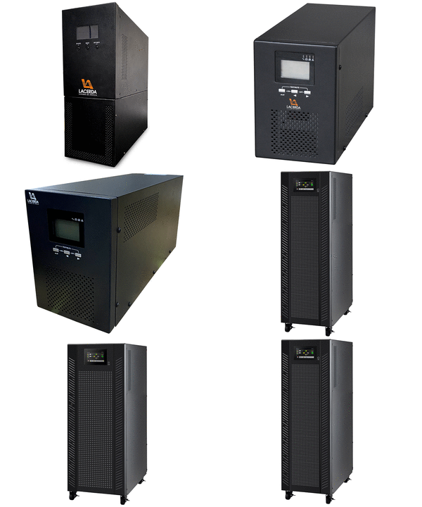
Desempenho Input Stage with Double Functionality Applied to a High Performance Three-Phase UPS William A. Venturini, Henrique Jank, Fábio E. Bisogno, Mário L. S. Martins, Humberto Pinheiro ESTÁGIO DE ENTRADA COM DUPLA FUNCIONALIDADE APLICADO A UMA UPS TRIFÁSICA DE ALTO DESEMPENHO William A. Venturini, Henrique Jank, Fábio E. Bisogno, Mário L. S. Martins, Humberto Pinheiro Universidade Federal de Santa Maria, Santa Maria – RS, Brasil e-mail: {williamventurini, hiquejank, fbisogno, mariolsm, humberto.ctlab.ufsm.br}@gmail.com
No Blog Eletrônica de Potência você encontrará informações sobre teses,artigos,seminarios,congressos,tecnologias,cursos,sobre eletrônica potência. “TEMOS O DESTINO QUE MERECEMOS. O NOSSO DESTINO ESTA DE ACORDO COM OS NOSSOS MERITOS” ALBERT EINSTEIN. Imagination is more important than knowledge, for knowledge is limited while imagination embraces the entire world. EL FUTURO SE CONSTRUYE HOY,EL SUCESSO NO ES FRUTO DE LA CASUALIDAD,SE HUMILDE ,APRENDE SIEMPRE CADA DIA.
AUTOR DO BLOG ENG.ARMANDO CAVERO MIRANDA SÃO PAULO BRASIL

.gif)
“GRAÇAS A DEUS PELA VIDA,PELA MINHA FAMÍLIA,PELO TRABALHO.PELO PÃO DE CADA DIA,POR NOS PROTEGER DO MAL”
“SE SEUS PROJETOS FOREM PARA UM ANO,SEMEIE O GRÂO.SE FOREM PARA DEZ ANOS,PLANTE UMA ÁRVORE.SE FOREM PARA CEM ANOS,EDUQUE O POVO”


https://picasion.com/


quarta-feira, 22 de janeiro de 2025
Input Stage with Double Functionality Applied to a High Performance Three-Phase UPS William A. Venturini, Henrique Jank, Fábio E. Bisogno, Mário L. S. Martins, Humberto Pinheiro ESTÁGIO DE ENTRADA COM DUPLA FUNCIONALIDADE APLICADO A UMA UPS TRIFÁSICA DE ALTO DESEMPENHO William A. Venturini, Henrique Jank, Fábio E. Bisogno, Mário L. S. Martins, Humberto Pinheiro Universidade Federal de Santa Maria, Santa Maria – RS, Brasil
Desempenho Input Stage with Double Functionality Applied to a High Performance Three-Phase UPS William A. Venturini, Henrique Jank, Fábio E. Bisogno, Mário L. S. Martins, Humberto Pinheiro ESTÁGIO DE ENTRADA COM DUPLA FUNCIONALIDADE APLICADO A UMA UPS TRIFÁSICA DE ALTO DESEMPENHO William A. Venturini, Henrique Jank, Fábio E. Bisogno, Mário L. S. Martins, Humberto Pinheiro Universidade Federal de Santa Maria, Santa Maria – RS, Brasil e-mail: {williamventurini, hiquejank, fbisogno, mariolsm, humberto.ctlab.ufsm.br}@gmail.com
terça-feira, 21 de janeiro de 2025
Isolated Single-stage Three-phase AC/DC Converter using Bidirectional Switches Ramandeep Narwal† , Isaac Wongx , Subhashish Bhattacharya‡ , B. Jayant Baliga§ and Douglas C. Hopkins∗ FREEDM Systems Center, Department of Electrical and Computer Engineering North Carolina State Univers
Isolated Single-stage Three-phase AC/DC Converter using Bidirectional Switches Ramandeep Narwal† , Isaac Wongx , Subhashish Bhattacharya‡ , B. Jayant Baliga§ and Douglas C. Hopkins∗ FREEDM Systems Center, Department of Electrical and Computer Engineering North Carolina State University Raleigh, NC 27695, USA
Abstract—The advent of the SiC Bidirectional FET (BiDFET), a monolithic 1.2 kV bidirectional switch, has rendered the single-stage three-phase AC/DC converter topology a promising approach for implementing AC/DC converters. This topology, which integrates a full-bridge converter with a single-phase to three-phase matrix converter via a high-frequency transformer, is particularly suitable for applications requiring galvanic isolation, buck-boost functionality, and bidirectional power flow. The single-stage design eliminates the need for bulky and unreliable electrolytic capacitors, and utilizes a single magnetic component for power transfer. In the matrix converter, bidirectional switches, which were traditionally implemented using combinations of multiple semiconductor devices such as MOSFETs, IGBTs, and diodes, can now be realized using the single-chip solution, BiDFET. This advancement leads to a lower switch count, compact converter implementation, with lower inductance commutation cells, thereby enhancing the overall efficiency and compactness of the system. The paper presents a unified model of the converter, considering all control parameters, including the duty cycles and phase shift of transformer voltages. Detailed expressions for power transfer, transformer currents, and currents at AC and DC ports are provided. Additionally, the paper outlines the conditions necessary for soft-switching of all switches and the commutation schemes required for the practical implementation of the matrix converter modulation scheme. A hardware prototype of a 10 kW, 480 VRMS, LL/ 800 V AC/DC system has been developed, and experimental results are presented to demonstrate its performance.
VIEW FULL PAPER: https://www.osti.gov/servlets/purl/2324747
Planar Transformer Systems for Modular Power Electronics in Long-Haul, Low-Cost PV Systems-Mike K. Ranjram Title: Assistant Professor-Arizona State University
Planar Transformer Systems for Modular Power Electronics in Long-Haul, Low-Cost PV Systems Mike K. Ranjram Title: Assistant Professor-Arizona State University
Design and Qualification of a 100 kW Three-Phase SiC-Based Generator Rectifier Unit Rated for 50,000 ft Altitude Jiewen Hu, Member, IEEE, Xingchen Zhao, Student Member, IEEE, Lakshmi Ravi, Student Member, IEEE, Rolando Burgos, Senior Member, IEEE, Dong Dong,
Design and Qualification of a 100 kW Three-Phase SiC-Based Generator Rectifier Unit Rated for 50,000 ft Altitude Jiewen Hu, Member, IEEE, Xingchen Zhao, Student Member, IEEE, Lakshmi Ravi, Student Member, IEEE, Rolando Burgos, Senior Member, IEEE, Dong Dong, Senior Member, IEEE, Richard Eddins, Sriram Chandrasekaran and Saeed Alipour
segunda-feira, 20 de janeiro de 2025
Optimal Design of MHz LLC Converter for 48V Bus Converter Application Yinsong Cai, Student Member, IEEE, Mohamed H. Ahmed, Student Member, IEEE, Qiang Li, Member, IEEE, and Fred C. Lee, Life Fellow, IEEE
Optimal Design of MHz LLC Converter for 48V Bus Converter Application Yinsong Cai, Student Member, IEEE, Mohamed H. Ahmed, Student Member, IEEE, Qiang Li, Member, IEEE, and Fred C. Lee, Life Fellow, IEEE


