AUTOR DO BLOG ENG.ARMANDO CAVERO MIRANDA SÃO PAULO BRASIL

"OBRIGADO DEUS PELA VIDA,PELA MINHA FAMILIA,PELO TRABALHO,PELO PÃO DE CADA DIA,PROTEGENOS DO MAL"

"OBRIGADO DEUS PELA VIDA,PELA MINHA FAMILIA,PELO TRABALHO,PELO PÃO DE CADA DIA,PROTEGENOS  DO MAL"

“SE SEUS PROJETOS FOREM PARA UM ANO,SEMEIE O GRÂO.SE FOREM PARA DEZ ANOS,PLANTE UMA ÁRVORE.SE FOREM PARA CEM ANOS,EDUQUE O POVO.”

“Sixty years ago I knew everything; now I know nothing; education is a progressive discovery of our own ignorance. Will Durant”

domingo, 24 de janeiro de 2010

Transfer Mold PFC Series with Compact Package


This article presents a new version of Mini Dual In-line Package Power Factor Correction
(DIPPFCTM) developed by Mitsubishi Electric Corporation for high power air conditioners
and general inverter use. In the new DIPPFC series, low thermal resistance was
realized by using an insulation sheet structure with high heat dissipation. Because of the
low thermal resistance, package size of the Mini DIPPFC is reduced compared to the
conventional large DIPPFC and input current rating is expanded up to AC 30Arms.
By Masahiro Kato, Teruaki Nagahara, Hisashi Kawafuji, Toshiya Nakano, Marco Honsberg
Power Device Works, Mitsubishi Electric Corporation, Japan
Configuration of DIPPFCTM
In recent years, high harmonic currents generated in electric power
systems are restricted in all electronic equipment. Especially in the
EU where IEC61000-3-2 is applied, the high harmonic current regula
tion are severe, and the application of PFC (Power Factor Correction)
is advanced. The power factor correction circuit shown in Figure
2 is now widely used. This circuit is composed of the diode bridge,
the switching device and the boost diode. In the DIPPFC, the highside
diode of the diode bridge has the function of boost diode, and
an IGBT is added in parallel with the low-side diode of the diode
bridge, as shown in Figure 3.
Therefore, DIPPFC has the functions of rectification and power factor
correction. DIPPFC includes a driver IC for the IGBTs as shown in
Figure 2.
New package structure
Figures 4 and 5 show cross-sectional drawings of a Mini DIPPFC
compared with a Large DIPPFC. DIPPFC (including DIPIPM) series
are simply made up of power chips (IGBTs, diodes), drive ICs and
assembly components (lead frame, Al/Au wire, resin, etc.). Bare
power chips and ICs are assembled directly on a lead frame and
connected by Al wire or Au wire, and then they are transfer molded.
Heat dissipation structure
In Large DIPPFC, the insulating layer between lead frame and builtin
heat-sink is formed by epoxy resin. In order to reduce the thermal
resistance, a ceramic-powder filler with high thermal conductivity was
incorporated in the epoxy resin However this technology has reached
its limits of insulation strength and heat dissipation through the epoxy
resin because of the fluidity properties of the filler.
To solve the problem, the new heat dissipation structure with insulating
resin sheet has been adopted in the Mini DIPPFC as shown in
Figure 5. The insulating resin sheet does not need very much fluidity,
in contrast to the epoxy resin, thus it is possible to increase the
amount of filler in the resin sheet. By using this resin sheet, the thickness
of the insulating layer can be thinner compared with that of the
epoxy resin isolation in the Large DIPPFC. Therefore, the thermal
dissipation can be improved considerably. As a result, the thermal
resistance was improved 35% compared to the Large DIPPFC (as
shown in Figure 6).
Compact Package size
Effective heat dissipation of the power chips is achieved by applying
the new heat dissipation structure with an insulating resin sheet,
thereby the power chip size could be shrunk appropriately. Through
Figure2


sexta-feira, 22 de janeiro de 2010

REDRESSEUR TRIPHASE REVERSIBLE


Département ou laboratoire:
Laboratoire d'Electrotechnique et d'Electronique Industrielle (LEEI)
Directeur de thèse:
Foch, Henri et Richardeau, Frédéric
Roux, Nicolas (2004) Nouveaux mécanismes de commutation exploitant les protections intégrées des semi-conducteurs de puissance. Application à la conception de convertisseurs statiques à commutation automatique. (New switching processes using the integrated protections of power semi-conductors : application to the development of static converters with self-switching process.)

Cette thèse présente un nouveau mécanisme de commutation qui a pour but d’intégrer la protection du semi-conducteur dans le principe même de commutation, afin de générer de nouveaux convertisseurs statiques. Il consiste en une transition auto-commandée qui se déroule à un niveau de courant ou de tension non nul. Elle peut être associée avec les commutations commandée ou spontanée permettant de passer de deux à cinq types de changement d’état d’une cellule de commutation. De nouvelles règles élémentaires de fonctionnement d’une cellule de commutation émergent alors. Vu le grand nombre d’interrupteurs possibles, une mé thodologie de synthèse de cellules admettant une réversibilité de source, dont les interrupteurs sont identiques, est présentée permettant de faire apparaître différentes solutions, dont deux semblent particulièrement intéressantes : les cellules onduleur et redresseur à disjonction, utilisant toutes deux le thyristor-dual disjoncteur. Ce dernier sert de support d’étude du principe de blocage automatique. Puis, le manuscrit se concentre sur l’étude de convertisseurs, associations de cellules élémentaires, faisant apparaître notamment le transformateur à courant continu et le redresseur triphasé réversible. Ce dernier fait l’objet d’un prototype industriel. Enfin, à partir du cahier des charges d’une chaîne éolienne, notre montage a été mis en concurrence avec ce qui se fait à l’heure actuelle en matière de raccordement au réseau, faisant apparaître un gain au niveau des pertes ainsi qu’un rendement énergétique supérieur. ABSTRACT : This thesis deals with a new switching process which integrates the semiconductor protection directly in the switching principle, in order to generate new static converters. It consists of a self-controlled transition which proceeds on a non-zero current or voltage level. It can be associated with controlled or naturally switching processes making it possible to go from two to five change of state types of a switching cell. So, new elementary operation rules of a switching cell emerge. Considering the great number of possible switches, a synthesis methodology of cells with a source reversibility, whose switches are identical, is presented making it possible to reveal various solutions, of which two seem particularly interesting : the self-breaking inverter and rectifier cells, both using the self-breaking thyristor-dual. This last is used as study support of the self-breaking principle. Then, the manuscript concentrates on the study of converters, associations of elementary cells, revealing in particular the DC-current transformer and the reversible threephase self-breaking rectifier. This last had been developed as an industrial prototype. Lastly, starting from the concept of a wind chain, our assembly has been compared with what is presently done as network converters, revealing lesser losses as well as a higher energetic efficiency.
LE THYRISTOR-DUAL DISJONCTEUR
Le thyristor-dual est un composant qui a été développé à Toulouse afin d’être le
pendant du thyristor comme son nom l’indique. Il associe un amorçage au zéro de la tension à
un blocage commandé. Il allie de nombreux avantages : c’est un composant réversible en
courant donc constitué de seulement trois couches donnant un composant rapide. Il bénéficie
du préconditionnement du transistor par les charges stockées dans la diode lors de sa
conduction. Il permet également d’envisager une intégration fonctionnelle à court terme.
Enfin, c’est un composant qui permet une bonne sûreté de fonctionnement du convertisseur
dans lequel il est monté.
Pour toutes ces raisons, nous l’avons choisi comme base de développement pour notre
premier interrupteur incluant une commutation automatique : le thyristor-dual disjoncteur.
Nous l’avons synthétisé en discret afin de l’étudier dans le cadre la conversion statique. Ce
chapitre a pour but de présenter ce composant ainsi que sa réalisation.
Nous présentons par la suite les deux cellules élémentaires à base de thyristor-dual
disjoncteur : l’onduleur et le redresseur à disjonction.
Nous nous intéressons ensuite aux propriétés de cet interrupteur, avec un éclairage
particulier sur la maîtrise du courant de disjonction en fonction des différents paramètres
extérieurs.
Enfin, nous présentons la réalisation d’un micro-disjoncteur conçu au LAAS, ainsi
qu’une étude sur la mise en parallèle de disjoncteurs électroniques.
II.1. PRINCIPE DU THYRISTOR-DUAL DISJONCTEUR
Le thyristor-dual disjoncteur est un thyristor-dual dont le blocage commandé a été
remplacé par un auto-blocage par surcourant. Le symbole de l’interrupteur ainsi que sa
caractéristique sont donnés à la Figure II-1. Le trait pointillé entre la diode et le transistor
représente l’amorçage spontané de ce dernier sous zéro de tension lorsque la diode se met à
Le thyristor-dual disjoncteur
conduire. Le composant s’amorce de manière naturelle par mise en conduction de la diode.
Durant sa conduction, le transistor est amorcé, le rendant potentiellement passant. C’est le
circuit extérieur qui impose alors le changement de signe du courant. A ce moment, le courant
transite de la diode au transistor sous tension nulle.


MODELISATION ELECTRIQUE ET ENERGETIQUE DES ACCUMULATEURS LITHIUM-ION.


L’INSTITUT NATIONAL POLYTECHNIQUE DE LORRAINE
En vue d'obtention du titre de
DOCTORAT DE L’INPL
Spécialité : Génie Electrique
par Matthieu URBAIN
Ingénieur de l'Ecole Nationale Supérieure d'Electricité et de Mécanique
Date de soutenance : 04 juin 2009


quinta-feira, 21 de janeiro de 2010

AFFIDABILITA’ E QUALITA’ DEL SERVIZIO ELETTRICO PER UTENTI


POLITECNICO DE TORINO-Ingegneria Elettrica-
relatore: Prof. Roberto Napoli
Negli ultimi anni l’Italia è stata caratterizzata da un incremento dei consumi di
energia elettrica sia nel settore industriale che nel settore terziario, inoltre si è
riscontrato, grazie allo sviluppo tecnologico, un aumento sostanziale degli
utilizzatori che fruttano componenti elettronici molto sensibili, come vedremo, ai
disturbi della rete in grado di provocare mal funzionamenti o addirittura la rottura
di tali componenti.
Un altro cambiamento radicale che ha sconvolto il panorama elettrico per quanto
riguarda la produzione e la vendita di energia elettrica, è stato la liberalizzazione
del mercato che ha portato all’introduzione di soggetti terzi come distributori di
energia ,a differenza di quanto capitava in passato, dove questo mercato era
gestito interamente da ENEL.
Queste condizioni, cioè una maggiore qualità del servizio e la comparsa di tanti
piccoli distributori, ha evidenziato la necessità di avere delle linee guida da
seguire per regolare i rapporti tra le varie parti; tale necessità è stata recepita sia da
A.E.E.G. che ha emanato le proprie regole in campo legislativo, sia dal CEI che
ha stabilito le regole tecniche per uniformare tutte quelle regole che erano state
emanate da ogni singolo distributore.
In questo elaborato faremo inizialmente una panoramica sulle principali cause che
inficiano la qualità dell’alimentazione, per poi passare ad una analisi dei principali
aspetti delle leggi e delle regole tecniche vigenti, evidenziando alcuni problemi e
proponendo alcune soluzioni non prese in considerazione da queste.

State of the Art in Medium Voltage Power Semiconductors


Recent technology advances in power electronics have been made by improvements in
controllable power semiconductor devices. Figure 2-3 and Figure 2-4 summarize the most
important power semiconductors on the market and their rated voltages and currents today [14],
[21]. The device characteristics for medium voltage power semiconductors are shown in Table
2-2 [28].
Metal Oxide Semiconductor Field Effect Transistors (MOSFET) and IGBTs have replaced
Bipolar Junction Transistors (BJT) almost completely. A remarkable development in
MOSFETs took place during the last years. Nowadays MOSFETs are available up to a
maximum switch power of about 100kVA [21].
Various new concepts of MOS-controlled thyristors such as the MOS-controlled thyristor
(MCT) and the MOS turn-off thyristor (MTO) have been presented but they do not have any
commercial applications.
Conventional GTOs are available with a maximum device voltage of 6kV in traction and
industrial converters (Table 2-2) [21], [28]. The high on state current density, the high blocking
voltages, and the possibilities to integrate an inverse diode are considerable advantages of
these devices. However, the requiring of bulky and expensive snubber circuits [92], [93] as
well as the complex gate drive are the reasons that GTOs are being replaced by IGCTs and
Gifts [21], [28]. Like GTOs, IGCTs are offered only as a presspack device. The symmetrcial
IGCT is offered by Mitsubishi with a maximum device voltage of 6.5kV (Table 2-2) [21], [28].
An increase of the blocking voltage of IGCTs and inverse diodes to 10kV is technically
possible today [21].
Due to the thyristor latching, a GTO structure offers lower conduction losses than an IGBT of
the same voltage class. To improve the switching performance of classical GTOs, gatecommutated
thyristors (GCTs) with a very little turn-off delay (about 1.5μs) have been
developed [90], [91]. New asymmetric GCT devices up to 10kV with peak controllable
currents up to 1kA have been manufactured but only those devices with 6kV and 6kA are
commercially available.
IGBTs were introduced on the market in 1988. IGBTs from 1.7kV up to 6.5kV with dc current
ratings up to 3kA are commercially available today (Table 2-2) [21], [28]. They have been
optimized to satisfy the specifications of the high-power motor drives for industrial and
traction applications. They are mainly applied in a module package due to the complex and
expensive structure of an IGBT presspack [28].
In IGBT modules, multiple IGBT chips are connected in parallel and bonded to ceramic
substrates to provide isolation. Both IGCTs and IGBTs have the potential to decrease the cost
of systems and to increase the number of economically valuable applications as well as the
performance of high-power converters, compared to GTOs, due to a snubberless operation at
higher switching frequencies (e.g. 500-1000Hz).
Figure 2-5 represents the typical converter voltage as a function of power ratings for both IGBT
and IGCT applications [28], [30], [31]. It can be seen that LV-IGBT modules are commercially
available with a maximum device voltage of 1700V on the entire low-voltage drive market (i.e.
up to 690V). On the other hand, MV-IGBT modules enable converter designs in a voltage range
from 1kV up to 7.2kV with a power range from 200kVA up to 7MVA (Figure 2-4) [28]. MVIGBT
modules have replaced GTOs in recent traction applications.
“IGBT presspacks are applied mainly in self-commutated High Voltage Direct Current
(HVDC) converters (e.g. HVDC light) where a redundant converter design is a main
requirement and each converter switch position consists of a series connection of many IGBTs
(e.g. n ≥ 10) [28].”

quarta-feira, 20 de janeiro de 2010

Comparing Transformer-based and Transformerless Uninterruptible Power Supplies

Robin Koffler is the General Manager for Riello UPS Ltd the UK subsidiary of Riello UPS (RPS S.p.A)

Choosing between transformer-based or transformerless uninterruptible power supplies may not be a simple ‘either/or’ decision, particularly above 10kVA. Both technologies have their place in today’s power protection scenarios but the key differences between them are: physical size, efficiency, noise output and the levels of input harmonic distortion that they generate.
Both uninterruptible power supply designs produce a tightly regulated source of uninterrupted power but they differ in the way they generate the dc voltage required by their inverters and their output stages.
Transformer-based Uninterruptible Power Supplies: until the early 1990s, the only design of online uninterruptible power supply was transformer-based. Nowadays, the design is still available but generally in larger sizes for UPS from eight to 800kVA. The most common applications for this are large industrial sites.
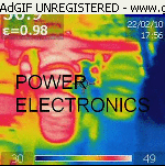
This type of UPS has a robust transformer-isolated inverter output, which makes it more suitable for the type of application where there is a likelihood of electrical noise; spikes, transients, and potentially, a high degree of short-circuit currents.
The inverter generates an ac supply from its dc power source, which is fed into a step-up transformer. The primary function of the transformer is to increase the inverter ac voltage to that required by the load. The transformer also protects the inverter from load disruption, whilst also providing Galvanic isolation (a method of isolating input and output).
Modern inverter designs use IGBTs (Insulated Gate Bipolar Transistors) in place of more traditional switching components (such as power transistors and thyristors). IGBTs combine the fast-acting and high power capability of the Bipolar Transistor with the voltage control features of a MOSFET gate to form a versatile, high frequency switching device. This in turn has given rise to more powerful, efficient and reliable inverters.
Transformer-based UPS are also supplied with a dual input option as standard, which can be selected at installation by simply removing a linking connector from its input terminal. This allows it to be powered from two separate ac supply sources thus adding further resilience. A transformerless UPS can be installed with dual input capability, with supplies derived from the same source, but this is typically a factory-fit option.
Transformerless Uninterruptible Power Systems
Transformerless UPS is a newer design, commonly available from 700VA to 120kVA. The primary purpose behind the introduction of transformerless units was to reduce the overall physical size and weight thus making an uninterruptible power supply unit more suitable for smaller installations and/or computer room/office type environments, where space may be limited. It also generates far less noise and heat than its transformer-based cousin and has far lower input harmonic distortion levels making it compatible with environments where electronic equipment (such as computers) may be more sensitive to this type of distortion.
In place of the step-up transformer, a transformerless UPS uses a staged process of voltage conversion. The first stage combines a rectifier and booster-converter to generate a dc supply for the inverter. An uncontrolled, three-phase bridge rectifier converts the ac supply into a dc voltage. This is passed through a mid-point booster circuit to step the dc voltage up to typically 700-800Vdc from which a battery charger and inverter are powered. In the second stage, the inverter takes the supply from the booster-converter and inverts it back to an ac voltage to supply the load.
An added benefit of this method is that the rectifier can operate from either a three or single-phase input supply. This can be configured at installation for systems up to 20kVA. A control system ensures a stable, regulated dc voltage is supplied to the inverter at all times and the inverter can operate regardless of UPS output load variations or mains power supply fluctuations or disturbances.
Choosing between Transformer-based or Transformerless Uninterruptible Power Supplies
In many applications the choice between the two may be clear. It is where the two ranges overlap, in terms of power rating, that the decision is more complicated. Consideration needs to be given then to: initial purchase cost, physical size, running costs, the installation environment, and in particular, the levels of input harmonic distortion they generate. Both designs can be operated in parallel to achieve higher levels of availability and resilience.
Over the last decade, the gap between these two uninterruptible power supply technologies has reduced as manufacturers have applied common techniques and research & development efforts to both designs. The driving force behind this has been cost and size, alongside demands to improve operating efficiency and reduce harmonic generation. In terms of online performance, both designs provide the same level of performance and are classified as VFI systems (voltage and frequency independent - in accordance with EN/IEC 62040-3). Their principal differences are their effects on upstream supplies and the operating environment.
Transformerless UPS are generally recognised as more efficient and having a higher power factor than an equivalent transformer-based design, therefore operating costs can be lower.
Below 10kVA, the transformerless UPS design dominates the online uninterruptible power supply market and has become the standard within data centre environments as they offer a more compact footprint, higher operating efficiencies and lower noise output. However, the strengths of the transformer-based design come into play in the industrial environment.

EXCELENTE ARTIGO DO ENG. ROBIN KOFFLER,ELE E REALMENTE VALIDO NOS MERCADOS EUROPEUS,NORTEAMERICANO,ASIATICO,MAIS NO MERCADO ESPECIFICAMENTE BRASILEIRO ,TERIA QUE TOMAR EM CONTA NOSSA REALIDADE ESPECIFICA,ISTO E,BRASIL E O CAMPEAO MUNDIAL DOS RAIOS,AS DESCARGAS ATMOSFERICAS NAS REGIONES SUDESTE E MAIOR PARTE DO TERRITORIO,SAO DE NATURALEZA INTENSA QUE OS UPS COM TRANSFORMADOR TEM MAIOR VIDA UTIL E ROBUSTEZ QUE OS QUE SAO PROJETADOS SEM TRANSFORMADOR,NESTE CASO OS CIRCUITOS SUPPRESSORES DE SURTOS E DESCARGAS ATMOSFERICAS TRABALHARAM A SUA MAXIMA CAPACIDADE,POR ISSO TEM QUE SER BEM ANALIZADO A ESCOLHA MAS CERTA PARA CADA NECESSIDADE.

SEMINARIO BASICO DE UPS


terça-feira, 19 de janeiro de 2010

DISPERSÃO DE TRANSFORMADORES DE BAIXA FREQUÊNCIA COMO FILTRO EM UMA UPS

V SEMINÁRIO NACIONAL
DE CONTROLE E AUTOMAÇÃO
INDUSTRIAL, ELÉTRICA E DE
TELECOMUNICAÇÕES


ESTUDO DE VIABILIDADE DA UTILIZAÇÃO DA DISPERSÃO DE TRANSFORMADORES DE
BAIXA FREQUÊNCIA COMO FILTRO EM UMA UPS DE 6kVA COM MODULAÇÃO PWM 3
NÍVEIS
Trabalho TT - 050 Página 1 de 5
Página 1 de 5
Halisson Alves de Oliveira *, Lucas Maciel Menezes *, Raphael Amaral da Câmara *, Cícero
Marcos Tavares Cruz *, Armando Walter Cavero Miranda **
* Universidade Federal do Ceará
** Microsol


RESUMO – Este artigo apresenta um estudo de
perdas no núcleo em um transformador de baixa
freqüência sendo alimentado por uma tensão
senoidal e por uma tensão em formato PWM
senoidal. As perdas no núcleo são comparadas
nos dois casos, sendo verificada a possibilidade
da utilização da dispersão do transformador como
elemento de filtro para um inversor com
modulação PWM senoidal de 6KVA. O estudo
visa também à redução de custos na UPS com a
retirada do indutor de filtro e utilização do
transformador como elemento filtrante,
isolamento galvânico e meio de elevação da
tensão de saída do inversor da UPS.
ABSTRACT – This paper presents a study of low
frequency power transformer losses with a
sinusoidal and a Pulse Width Modulation
sinewave input voltage in a commercial UPs. Two
cases are compared, the first one is a inverter
with PWM control technique with a LC filter and
after a low frequency power transformer. The
second case is the transformer connected directly
in the inverter output without the LC filter. The
study motivation is lower the UPS cost with the
LC filter removed, without any output voltage distortion.
READ FULL PAPER HERE

TÉCNICAS DE CONTROL ROBUSTO BASADO EN MODELO DE REFERENCIA APLICADAS A SISTEMAS MODULARES DE ALIMENTACION


TESIS DOCTORAL DEPARTAMENTO DE INGENIERÍA ELECTRÓNICA UNIVERSIDAD POLITÉCNICA DE VALENCIA AUTOR: MARCOS PASCUAL MOLTÓ. DIRECTOR: GABRIEL GARCERÁ SANFELIU.OCTUBRE 2007.

Parallel converter systems are an interesting solution to the problem of providing a tightly regulated output voltage at high current levels. Paralleling of converters allows for equal sharing of the load current betweenmodules. In this way, the stress in the semiconductor switches is reduced and reliability is improved.
In multimodule parallel converter systems, a current mode control scheme, like average current mode control (ACC), is usually needed in order to share the current between modules. In this scheme the control loop dynamic characteristicsdepend strongly on the line and load conditions, and also on the number of modules on stream.
In this thesis two different robust model-following (RMF) control techniques have been applied to parallel converter systems in order to improve the robustness of the ACC control. This work has been carried out in three different steps:
In first place, a high-pass RMF control scheme has been presented and applied to the voltage loop of a parallel Buck DC-DC converter. The proposed scheme adds a inner loop to the conventional current and voltage ACC loops, reducing the sensitivityof the outer voltage loop to the changing power stage parameters: number of modules, input voltage, load and component tolerances. Also, the loop improves significantly the disturbance rejection of the converter, i.e. the closed loop output impedance and audiosusceptibility, at low frequencies in comparison with conventional ACC.