sábado, 6 de fevereiro de 2010
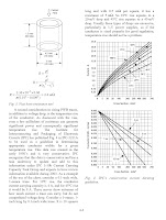
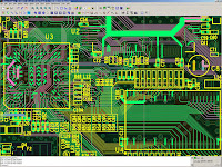
Constructing Your Power Supply- Layout Considerations


Robert Kollman
ABSTRACT
Laying out a power supply design is crucial for its proper operation; there are many issues to consider
when translating a schematic into a physical product. This topic addresses methods to keep circuit
parasitic components from degrading the operation of your designs. Techniques to minimize the impact
of parasitic inductance and capacitance of filter components and printed wire board (PWB) traces is
discussed, together with a description of the impact that PWB trace resistance can have on power
supply regulation and current capacity. A general overview of thermal design is also included as well as
sample temperature rise calculations in a natural and forced-air environment. Finally, some practical
examples of power stage and control device layouts are reviewed.
sexta-feira, 5 de fevereiro de 2010
Photovoltaic converter topologies suitable for SiC-JFETs
Benjamin Sahan, Samuel V. Araújo, Thomas Kirstein, Lucas Menezes, Peter Zacharias
Kompetenzzentrum für Dezentrale Elektrische Energieversorgungstechnik (KDEE),
University of Kassel, Wilhelmshöher Allee 71, D-34121 Kassel, b.sahan@uni-kassel.de
Abstract
SiC semiconductors offer very interesting characteristics and can be considered as a future trend in
photovoltaic converter technology. The vertical JFET is an example of a very promising device, mainly
due to its relative structural simplicity. Nevertheless, its inherent normally-on characteristic calls for
specially tailored topologies that will be presented and discussed in this publication.
READ FULL TEXT HERE
Assinar:
Postagens (Atom)



















 JOSIL ARTISTA PLASTICO FORTALEZA CEARA BRASIL AV.HERACLITO GRAÇA 41 TEL(85)32542378