sexta-feira, 31 de março de 2017
A PSR single-stage flyback LED driver with simple line regulation and quasi-resonant operation Nie Weidong(聂卫东) 1; 2; Ž, Yu Zongguang(于宗光) 1 , Wang Haibing(王海兵) 2 , Guo Bin(郭斌) 2 , Teng Long(滕龙) 2 , and Yang Lihang(杨力航) -Department of Electronic Engineering, Jiangnan University China
Abstract:
A single-stage flyback driving integrated circuit (IC) for light-emitting diodes (LEDs) is proposed. With an average primary-side current estimation and negative feedback networks, the driver operates in the boundary conduction mode (BCM), while the output current can be derived and regulated precisely. By means of a simple external resistor divider, a compensation voltage is produced on the ISEN pin during the turn-on period of the primary MOSFET to improve the line regulation performance. On the other hand, since the delay time between the time that the secondary diode current reaches zero and the turn-on time of the MOSFET can be automatically adjusted, the MOSFET can always turn on at the valley voltage even if the inductance of the primary winding varies with the output power, resulting in quasi-resonant switching for different primary inductances. The driving IC is fabricated in a Dongbu HiTek’s 0.35 m bipolar-CMOS-DMOS process. An 18 W LED driver is finally built and tested. Results show that the driver has an average efficiency larger than 86%, a power factor larger than 0.97, and works under the universal input voltage (85–265 V) with the LED current variation within 0.5%.
VIEW FULL TEXT
http://www.jos.ac.cn/bdtxben/ch/reader/create_pdf.aspx?file_no=13122603
LINK ALTERNATIVO
http://www.mediafire.com/file/85fyffk0jdxtehq/A_PSR_single-stage_flyback_LED_driver_with_simple_line_regulation.pdf
A Single-Stage High-Power-Factor Light-Emitting Diode (LED) Driver with Coupled Inductors for Streetlight Applications - Chun-An Cheng, Chien-Hsuan Chang, Hung-Liang Cheng , Ching-Hsien Tseng and Tsung-Yuan Chung-Department of Electrical Engineering, I-Shou University,TAIWAN
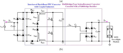
A Single-Stage High-Power-Factor Light-Emitting Diode (LED) Driver with Coupled Inductors for Streetlight Applications Chun-An Cheng, Chien-Hsuan Chang, Hung-Liang Cheng *, Ching-Hsien Tseng and Tsung-Yuan Chung Department of Electrical Engineering, I-Shou University, Dashu District, Kaohsiung City 84001, Taiwan;
Abstract:
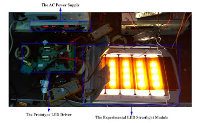
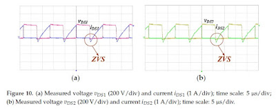
This paper presents and implements a single-stage high-power-factor light-emitting diode (LED) driver with coupled inductors, suitable for streetlight applications. The presented LED driver integrates an interleaved buck-boost power factor correction (PFC) converter with coupled inductors and a half-bridge-type series-resonant converter cascaded with a full-bridge rectifier into a single-stage power conversion circuit. Coupled inductors inside the interleaved buck-boost PFC converter sub-circuit are designed to operate in discontinuous conduction mode (DCM) for achieving input-current shaping, and the half-bridge-type series resonant converter cascaded with a full-bridge rectifier is designed for obtaining zero-voltage switching (ZVS) on two power switches to reduce their switching losses. Analysis of operational modes and design equations for the presented LED driver are described and included. In addition, the presented driver features a high power factor, low total harmonic distortion (THD) of input current, and soft switching. Finally, a prototype driver is developed and implemented to supply a 165-W-rated LED streetlight module with utility-line input voltages ranging from 210 to 230 V.
View Full-Text :
http://www.mdpi.com/2076-3417/7/2/167/pdf
A Single-Stage LED Tube Lamp Driver with Power-Factor Corrections and Soft Switching for Energy-Saving Indoor Lighting Applications Chun-An Cheng Department of Electrical Engineering Taiwan
Abstract:
This paper presents a single-stage alternating current (AC)/direct current (DC) light-emitting diode (LED) tube lamp driver for energy-saving indoor lighting applications; this driver features power-factor corrections and soft switching, and also integrates a dual buck-boost converter with coupled inductors and a half-bridge series resonant converter cascaded with a bridge rectifier into a single-stage power-conversion topology. The features of the presented driver are high efficiency (>91%), satisfying power factor (PF > 0.96), low input-current total-harmonic distortion (THD < 10%), low output voltage ripple factor (switching (ZVS) obtained on both power switches. Operational principles are described in detail, and experimental results obtained from an 18W-rated LED tube lamp for T8/T10 fluorescent lamp replacements with input utility-line voltages ranging from 100 V to 120 V have demonstrated the functionality of the presented driver suitable for indoor lighting applications.
LINK ORIGINAL View Full-Text
http://www.mdpi.com/2076-3417/7/2/115/pdf
quinta-feira, 30 de março de 2017
LED lighting control driver design and development of the 12V‐12W class using the voltage controlled ring oscillator - Ki-Soo Kwon Department of Electronic Engineering Graduate School Yeungnam University
LED lighting control driver design and development of the 12V‐12W class using the
voltage controlled ring oscillator
Ki-Soo Kwon
Department of Electronic Engineering
Graduate School
Yeungnam University
Abstract
This paper presents a Pulse Width Modulation (PWM) controller and circuits for the high power LED (Light Emitting Diode) driver. The controller is available for the remote control through four major operation modes of ON, OFF, Emergency and Power saving using the serial communication. The entire driver circuits use a DC‐DC converter such a Boost topology with dimming, current, thermal control and communication functions for hallway lighting and automobile applications. According to the type and power of LED, a driver IC has already been developed and is produced. This driver IC makes the constant current and constant voltage available. However, if the LED driver allows delicate dimming control and thermal dissipation through allowance of LED off time, PWM control is needed. Therefore, a MCU (Microcontroller unit) for the PWM control as well as a driver IC for driving LEDs is needed. If this operation is embedded at this driver IC, the expense can be reduced. The LED controller integrated circuit (IC) was designed, simulated and fabricated in 0.35μm Magnachip/Hynix.
terça-feira, 28 de março de 2017
An Electrical Method for Junction Temperature Measurement of Power Semiconductor Switches- Baker, Nick -Aalborg Universy-DENMARK
Dissertation submitted: April 6th 2016 PhD supervisor: Prof. Stig Munk-Nielsen Aalborg University, Denmark PhD
committee: Professor Josep Guerrero (chairman) Aalborg University Dr. Gernot J. Riedel ABB Cooperate Research Professor Philip Andrew Mawby University of Warwick PhD Series: Faculty of Engineering and Science, Aalborg University
Abstract
Power semiconductor switches are critical components in power electronic converters and operate in thermally stressful environments. The junction temperature of a power semiconductor directly influences its power loss and is intrinsically linked to numerous failure mechanisms. Knowledge of this temperature is therefore important for optimal operation and for reliability reasons. If the junction temperature is known during the operation of a converter, real-time condition monitoring and active thermal control systems could be developed to improve system reliability. Performing direct measurements of junction temperature is difficult since the power semiconductor is generally encapsulated inside an array of packaging materials. Alternatively, the electrical behaviour of a semiconductor largely depends on temperature. If this relationship is known, the electrical parameters of the device can be monitored and used to estimate the junction temperature. These are known as Temperature Sensitive Electrical Parameters (TSEPs) and are one way to carry out non-invasive, real-time junction temperature measurements on fully packaged devices. Nevertheless, successful implementation of these techniques during the normal operation of a power semiconductor is thus far limited. Often holding back their use is the need to compensate for inherent fluctuations caused by a constantly changing electrical environment (or alternatively requiring interruption to normal operation to force fixed electrical conditions), and significant uncertainty over accuracy. As a result, this PhD aims to develop new methods, or improvements to existing methods, for junction temperature measurement via TSEPs during the operation of power semiconductor switches. In Chapter 1, the state-of-the-art in the topic of junction temperature measurement is introduced. A literature review of TSEPs investigated for use in operating power semiconductor switches is then provided. From this, several implementation issues are identified and used to formulate technical objectives for the PhD thesis. Chapter 2 introduces the first original contribution of the thesis. Two TSEP-based methods for junction temperature measurement, unpublished in scientific literature before the commencement of the PhD, are presented. The measurement principles are explained, and experimental validation is provided on Insulated-Gate-Bipolar-Transistors (IGBTs). The foremost advantages in the presented TSEPs are that they are measured without interruption to normal IGBT operation, and do not require compensation for varying load current conditions. The primary method presented is referred to as the Peak Gate Current (IGPeak) method, which is selected for further examination in Chapter 3. In Chapter 3, the second scientific contribution of the thesis is provided. Here, the accuracy of the IGPeak method on IGBTs is extensively examined using direct measurements of junction temperature from an Infra-Red camera. The validation is performed on IGBT dies with differing geometry, as well as IGBTs in both healthy and degraded conditions. Finally, IGBTs in a paralleled configuration are investigated. These results in terms of accuracy are compared with a traditional TSEP method commonly found in prior art.
LINK ORIGINAL
http://vbn.aau.dk/files/240989038/PHD_Nick_Baker_E_pdf.pdf
Assinar:
Postagens (Atom)













 JOSIL ARTISTA PLASTICO FORTALEZA CEARA BRASIL AV.HERACLITO GRAÇA 41 TEL(85)32542378