


sábado, 14 de março de 2020
quinta-feira, 12 de março de 2020
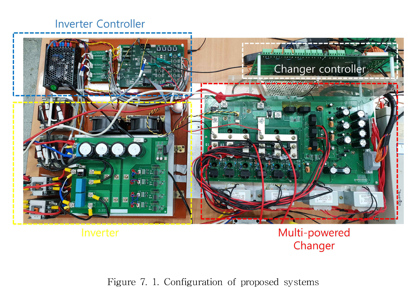
Multi-powered UPS Master's Thesis-KIM Jongcheol Department of Electrical Engineering Graduate School, Chonnam National University
Department of Electrical Engineering Graduate School, Chonnam National University
Author KIM Jongcheol
Supervised by Professor Park Sungjun
A dissertation submitted in partial fulfillment of the requirements for the Master's Thesis in Electrical Engineering
(Abstract) As the society develops, load sensitive to power environment such as medical equipment, communication equipment, FA (factory automation) system and data center server is widely used, and reliability and stable supply of power system becomes more important. In particular, electrical equipment used for military purposes is not expected to have any problems in the power supply system during exhibition or operation, so it is becoming necessary to secure a reserve energy source, to duplicate the system or to make surplus system. Even if the reliability of the power supply system is high, momentary power failure due to an accident or a lightning can not be avoided, and there is also a momentary voltage drop (Sag) or a voltage rise (swell) of the power supply. Table 1 below is a definition of the power anomaly phenomenon that appears in the commercial power source shown in IEEE Std 1159TM-2009. In case of power-sensitive load, it is necessary to prepare for system failure because it can cause fatal damage even in short-term system failure. Therefore, there is a need for an uninterruptible power supply (UPS) [1] [2] to compensate for instantaneous voltage fluctuations as well as for blackout situations. Automotive UPS systems typically consist of a single module, such as a battery, bi-directional inverter, high-speed switch, and the UPS module is connected to the vehicle generator and critical loads. If the existing UPS system is composed of a single power source and the UPS system is composed of only one power source, it is difficult to cope with the demand of the main load in the long term only by the output of the UPS when the power source is out of power. To solve this problem, connecting several power sources to a load leads to a large increase in cost due to the connection of UPS to each power source. It is an off-line UPS system that is commonly used. The advantage of the off-line method is that when the input power is normal, there is less generation of electromagnetic waves and noise, and the power consumption is low due to high energy efficiency. In addition, it has a simple circuit configuration, high durability, low cost, and miniaturization compared to on-line. The disadvantage of off-line is that momentary power cut-off occurs in the case of power failure, and the output changes according to the input voltage change during non-operation, making it difficult to adjust the voltage and therefore it is not suitable for high-precision load. In the case of Figure 1, it is composed of a single power source, and if the UPS system consists of only one power source, it is difficult to cope with the demand of the main load in the long term only by the output of the UPS when the power source is outage. In particular, in a system having a purpose for use in a command communication terminal of a military, it is difficult to supply stable power because there are many variables in power supply. In this paper, we propose a multi - power applied UPS system that eliminates the disadvantages of the parallel - connected power supply and has a fast switching time. The UPS system operates in the battery charging mode when the system is in normal operation and operates in the UPS mode, which is the battery discharge mode, in the event of a system failure. In such a mode switching, the follow up of the command voltage should be performed within the shortest time. Since the UPS must supply the same voltage to the load within 4ms in case of a system fault, the switching time and return time must be short when controlling the output voltage and current of the UPS, and the power failure detection time is also important. In addition, since the main loads of the UPS system are mostly time-varying and non-linear loads, it is also necessary to be able to control non-linear loads. Conventionally, a proportional integral (PI) controller has been used as a control method of such a UPS system. The PI controller has a very stable output characteristic in the steady state, but it takes a long time to reach the steady state at the time of mode change or load change due to slow acceleration. Therefore, due to the limit of the transient response characteristic of the controller, it is difficult to perform stable power supply within a short time in the case of a system fault. Also, since the gain of the PI controller affects the response characteristics, response characteristics may be slow or overshoot may occur depending on the gain value selection of the controller. Therefore, in this paper, to compensate the limitation of the proportional integral controller, the controller using the DFT with fast electrostatic sensing characteristics is applied. The control using DFT has an advantage that it can perform fast power failure detection by comparing grid voltage waveform and voltage waveform created by DFT using Schmitt trigger. Therefore, stable power supply is possible when using only PI control in mode switching in UPS system. The multi-power applied UPS system proposed in this paper is finally designed to satisfy the following conditions. In case of system fault, detection method using fast DFT is applied to the electrostatic detection in order to supply stable power to the load in a shorter time than the conventional PI control method. At this time, the switching time of mode switching was set to be less than 4 ms, which is 1/4 of the system cycle, according to KS C 4310 regulation of the uninterruptible power supply in the industry standard council. A 10kW UPS system, in which commercial voltage, vehicle generator, and auxiliary diesel generator can be connected to the proposed switchgear, was tested and validated.
LINK: http://www.mediafire.com/file/zoxi1y6ul1tfkov/MULTIPOWERED.pdf/file
quinta-feira, 5 de março de 2020
Estudio comparativo de un convertidor CC-CC en puente completo con dispositivos semiconductores basados en silicio y en nitruro de galio-Gómez Méndez, Álvaro (2016).-E.T.S.I. Industriales (UPM)


Title Estudio comparativo de un convertidor CC-CC en puente completo con dispositivos semiconductores basados en silicio y en nitruro de galio
Author/s Gómez Méndez, Álvaro
Contributor/s Uceda Antolín, Javier Molina, José María
Abstract
El objetivo de este TFG es desarrollar 2 convertidores CC-CC en puente completo controlado con la técnica de desfase entre ramas o phase-shift, utilizando dispositivos de Silicio (Si) y de Nitruro de Galio (GaN). Los dispositivos de Silicio son muy comunes en las fuentes de alimentación auxiliares, mientras que los de Nitruro de Galio, son relativamente nuevos, y su estudio presenta un gran atractivo de cara a las futuras fuentes de alimentación, por sus características, que permiten aumentar la densidad de potencia de las mismas. En este trabajo, ambos convertidores serán controlados mediante la SpCard (herramienta de prototipado rápido), con el fin de comparar estas dos tecnologías. Este TFG pretende valorar las ventajas de emplear componentes de GaN en el diseño de convertidores continua-continua de baja potencia, además de valorar las dificultades añadidas en el diseño como consecuencia del aumento de la frecuencia de conmutación, especialmente empleando un sistema de prototipado rápido como la SpCard. Para ello, en primer lugar se ha comenzado por un análisis de la topología en cuestión para comprender su funcionamiento con detalle. El convertidor de puente completo, ampliamente conocido como Full-Bridge, es un convertidor CC-CC con aislamiento galvánico, y está formado por un condensador de entrada, un puente inversor de transistores, un transformador de alta frecuencia para proporcionar dicho aislamiento galvánico, un puente rectificador de diodos y un filtro LC de salida. Su funcionamiento básico es el siguiente: La corriente continua de entrada se transforma en alterna de onda cuadrada en el puente inversor ya que, cuando conducen los transistores M1 y M4 a la vez se aplica una tensión positiva al primario del transformador; negativa cuando conducen M2 y M3; y nula en el resto de los casos. En el transformador se le aplica la relación de transformación además de desacoplar galvánicamente primario de secundario. En el rectificador, la onda cuadrada negativa se hace positiva, resultando en una corriente positiva pulsada. Por último, esta corriente pulsada se transforma en continua en el filtro LC. Las pérdidas de este circuito se deben fundamentalmente a dos tipos: conducción y conmutación. Sin embargo, las pérdidas por conmutación se pueden reducir considerablemente si la tensión y la intensidad no conviven en el momento en el que se produce una conmutación. Este fenómeno se denomina soft-swiching. Este circuito favorece su funcionamiento bajo soft-switching en el encendido de los interruptores, lo que se denomina ZVS (Zero Voltage Switching) o "conmutación a tensión nula", de forma natural bajo ciertas condiciones, debido a los elementos parásitos de los componentes que lo forman. Para favorecer este fenómeno, mediante la técnica de phase-shift o desplazamiento de fase entre ramas, se introduce un pequeño retardo entre los disparos de una rama y la otra del puente inversor, siendo los disparos de una misma rama complementarios. Se procede al diseño de dos convertidores: uno con transistores de Si (MOSFETs) a 200 KHz, y otro con transistores de GaN (eGaN FETs) a 1 MHz. Ambos funcionan con una tensión de 12 V de entrada, 5 V de salida y una potencia máxima de 30 W. Se calculan las inductancias y capacidades del filtro de salida para ambos convertidores, así como la relación de transformación del transformador. A continuación, se diseña el circuito de control. El siguiente paso consiste en añadir un circuito de medida de la tensión de salida y la corriente entre el condensador de entrada y el puente inversor, que posibilite la realimentación a la SpCard, habilitando la posibilidad del cierre del lazo de control en un futuro. Una vez desarrollado el esquemático, se diseña un transformador para 1MHz y otro para 200KHz mediante el software Pexprt. El siguiente paso consiste en realizar simulaciones de ambos diseños para comprobar que todo funciona de forma correcta antes de continuar con el desarrollo de estos. A continuación se seleccionan los componentes para ambos circuitos y se procederá al diseño de la PCB de eGaN FETs mediante el software Altium.
LINK:http://oa.upm.es/43788/1/TFG_CARLOTA_LOPEZ_PEREZ_ARROYO.pdf
quarta-feira, 4 de março de 2020
Diseño, fabricación y validación de fuentes de alimentación. Proyecto Fin de Carrera-Rodríguez Molina, Alberto (2018)-E.T.S.I. Diseño Industrial (UPM), Madrid.


Abstract
El trabajo consiste en el diseño e implementación de 3 convertidores buck con distintos controladores, y su posterior comprobación de que cumple con los requisitos impuestos al iniciar el proyecto. A partir de las hojas de características de estos controladores, se ha realizado un cálculo y un diseño esquemático del circuito electrónico para luego, posteriormente, llevar a cabo una simulación del comportamiento del convertidor. Una vez son favorables los resultados de dicha simulación, se lleva a cabo el diseño de la PCB y una vez finalizado y enviado a fabricar, se comprueban que los resultados concuerdan con los vistos en las simulaciones. Para llevar a cabo este proceso se ha requerido unos paquetes de software para la simulación del comportamiento como para el diseño de la PCB, además de la instrumentación necesaria para validar los requisitos impuestos en el proyecto.
LINK:http://oa.upm.es/49659/1/TFG_ALBERTO_RODRIGUEZ_MOLINA.pdf


Assinar:
Postagens (Atom)


 JOSIL ARTISTA PLASTICO FORTALEZA CEARA BRASIL AV.HERACLITO GRAÇA 41 TEL(85)32542378