CONVERTERS FOR RENEWABLE ENERGY APPLICATIONS by AHMAD SAEED Y. ALZAHRANI MISSOURI UNIVERSITY OF SCIENCE AND TECHNOLOGY
terça-feira, 16 de novembro de 2021
ADVANCED TOPOLOGIES OF HIGH-VOLTAGE-GAIN DC-DC BOOST CONVERTERS FOR RENEWABLE ENERGY APPLICATIONS by AHMAD SAEED Y. ALZAHRANI--MISSOURI UNIVERSITY OF SCIENCE AND TECHNOLOGY--DOCTOR OF PHILOSOPHY in ELECTRICAL ENGINEERING 2018
CONVERTERS FOR RENEWABLE ENERGY APPLICATIONS by AHMAD SAEED Y. ALZAHRANI MISSOURI UNIVERSITY OF SCIENCE AND TECHNOLOGY
In Partial Fulfillment of the Requirements for the Degree
DOCTOR OF PHILOSOPHY
in
ELECTRICAL ENGINEERING- 2018
ABSTRACT
This dissertation proposes several advanced power electronic converters that are
suitable for integrating low-voltage dc input sources, such as photovoltaic (PV) solar panels,
to a high voltage dc bus in a 200 − 960 V dc distribution system. The proposed converters
operate in the continuous conduction mode (CCM) and offer desirable features such as lowvoltage stresses on components, continuous input currents, and the ability to integrate several
independent dc input sources. First, a family of scalable interleaved boost converters with
voltage multiplier cells (VMC) is introduced. Several possible combinations of Dickson
and Cockcroft-Walton VMCs are demonstrated and compared in terms of the voltage gain,
number of components, and input current sharing. This dissertation also presents a novel
VMC structure called Bi-fold Dickson. The novel VMC offers equal current sharing between
phases regardless of the number of stages, voltage ripple cancellation at each stage, and
does not require an output diode. A family of high-voltage-gain multilevel boost converters
is presented, with detailed example of the hybrid flyback and three-level boost converter.
In this family, the effective frequency seen by the magnetic element is multiple times
the switching frequency, and therefore smaller magnetic devices can be used. Theory of
operations, steady-state analysis, component selections, simulation, and efficiency analysis
are included for each proposed converter. The operation of the proposed converters was
further verified with 80 − 200 W hardware prototypes.
segunda-feira, 15 de novembro de 2021
Design and Control Methodology for Improved Operation of a HV Bipolar Hybrid Switched Capacitor Converter J. Delhotal, J. Richards, J. Stewart, J. Neely, J. Flicker, R. Brocato, L. Rashkin Sandia National Laboratories Albuquerque, New Mexico, USA
Design and Control Methodology for Improved Operation of a HV Bipolar Hybrid Switched Capacitor Converter J. Delhotal, J. Richards, J. Stewart, J. Neely, J. Flicker, R. Brocato, L. Rashkin Sandia National Laboratories Albuquerque, New Mexico, USA Email: jneely@sandia.gov Jane Lehr University of New Mexico Albuquerque, New Mexico, USA
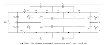
Abstract— In this work, a novel dc-dc converter topology, an
adaptation of the Hybrid Switched Capacitor Circuit (HSCC), is
considered for use in high-gain, high voltage applications that
also require high efficiency and superior power density. In
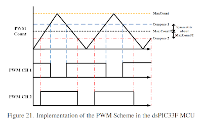
particular, a bipolar HSCC design is described, and a candidate
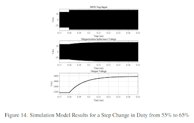
control methodology is set forth and developed analytically. The
converter performance is demonstrated to be consistent with
analysis. In addition, the converter is demonstrated to step 460V
up to 8.63 kV (gain of 19) at 3.63 kW and nearly 97.0%
efficiency.
LINK VIEW FULL TEXT IN WEB:
DESIGN AND DEVELOPMENT OF POWER PROCESSING UNITS FOR APPLICATIONS IN ELECTRICALLY-PROPELLED SATELLITE SYSTEMS by KARTIKEYA JAYADURGA PRASAD VEERAMRAJU---Requirements for the Degree MASTER OF SCIENCE in ELECTRICAL ENGINEERING--MISSOURI UNIVERSITY OF SCIENCE AND TECHNOLOGY-
DESIGN AND DEVELOPMENT OF POWER PROCESSING UNITS FOR APPLICATIONS IN ELECTRICALLY-PROPELLED SATELLITE SYSTEMS by KARTIKEYA JAYADURGA PRASAD VEERAMRAJU
A THESIS
Presented to the Graduate Faculty of the
MISSOURI UNIVERSITY OF SCIENCE AND TECHNOLOGY
In Partial Fulfillment of the Requirements for the Degree
MASTER OF SCIENCE
in
ELECTRICAL ENGINEERING
2020
ABSTRACT
Electrospray technology provides a way to ionize specialized liquids by applying
high voltages across a sharp porous tip and a metallic mesh. This technology is widely
used in the field of mass spectroscopy for generating ions for testing purposes. The dawn of
nano-satellites posed new challenges in the miniaturization of many conventional satellite
sub-systems. One significant challenge faced in such a process was the miniaturization
of the propulsion system. Electrosprays have started to find their application in the field
of Aerospace Engineering and now are formally known as Electrospray Thrusters. These
thrusters provide high specific impulse and are attractive substitutes to conventional gas
propelled thrusters as they can be scaled down in size and can also provide extended
mission times. Some of the new challenges faced in such applications are the generation of
high voltages from a lowvoltage onboard battery, grounding, spacecraft charging, clearance,
and reliability issues for long term usage.
In this work, a complete design process is developed for the realization of such high
voltages suitable for interfacing with an electrospray thruster. Simulation models for a new
type of converter are assessed, and its feasibility is discussed. A hardware prototype is
implemented, and the practical results are assessed.
An analysis of the converter is presented, and the semiconductor and passive components
are selected. Magnetic components are designed based on the analysis. Parallels
are drawn between the theoretical and prototype model of the concept converter.
Finally, the firmware of the converter is explained, and the communication protocol
of the PPU is delineated. As the boards designed for the converter have to sustain high voltages
and reliably operate in unfavorable environments, special PCB layout considerations
must be used, which also forces a designer to look for various other materials for the PCB
fabrication.
LINK VIEW FULL TEXT IN WEB:
sábado, 6 de novembro de 2021
Characterization and Design of HighSwitching Speed Capability of GaN Power Devices in a 3-Phase Inverter-Rémi PERRIN-THESE de DOCTORAT DE L’UNIVERSITE DE LYON opérée au sein de Laboratoire AMPERE
Characterization and design of the switching frequency rise of a 3-phase inverter with GaN transistors by Rémi Perrin
Abstract
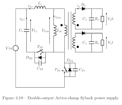
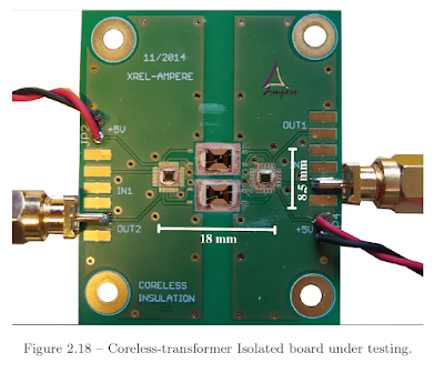
The French industrial project MEGaN aims to develop a power module based on HEMT compost in GaN. One of the industrial applications concerns aeronautics with a high constraint in galvanic isolation (> 100 kV / s) and in ambient temperature (200 ° C). The thesis work was focused on a power module brick (650 V 30 A inverter arm). The objective is to achieve a prototype of thin form factor, 30 cm2 and embedding all the driver functions, driver power supply, bus capacity and phase current sensor. This objective implies high energy efficiency, and respect for galvanic insulation while the surface stress is high. The manuscript, in addition to the state of the art relating to the power module and in particular that based on GaN HEMT transistor, discusses a micro-transformer-based control signal isolation solution. Micro-transformer prototypes were characterized and aged for 3000 hours to assess the robustness of the solution. The work contributed to the characterization of several GaN components in order to mature models for circuit simulation of converter topology. Within the MEGaN collaborative work, our contribution did not concern the design of the integrated circuit (grid driver), while having participated in the validation of the specifications, but a power supply strategy for the grid driver. A first isolated power supply proposal for the gate driver favored the use of low-voltage GaN components. The resonant flyback topology with clamp makes it possible to get the most out of these GaN components but poses the constraint of the power transformer. Several technologies for the realization of the transformer have been validated experimentally and in particular an original proposal for the burial of the magnetic component within a high-temperature polymer substrate. In particular, an inexpensive manufacturing process makes it possible to obtain a reliable device (1000 h of cycling between - 55; + 200 ° C), with an intrinsic efficiency of 88% for 2 W transferred. The parasitic insulation capacity is reduced compared to previous prototypes. Two prototypes of highly integrated power supplies use either low voltage GaN transistors (2.4 MHz, 2 W, 74%, 6 cm2), or a dedicated integrated circuit in CMOS SOI technology, designed for the application (1.2 MHz, 2 W, 77%, 8.5 cm2). The manuscript then proposes an integrable solution for measuring the phase current of the bridge arm, based on a magnetoresistance. The experimental comparison with respect to a shunt resistance solution. Finally, two converter prototypes are described, one of which has been the subject of an experimental validation demonstrating reduced switching losses.
VIEW FULL TEXT :http://theses.insa-lyon.fr/publication/2017LYSEI001/these.pdf
Design and characterization of a three-phase current source inverter using 1.7kV SiC power devices for photovoltaic applications-Présentée par Luís Gabriel ALVES RODRIGUES Laboratoire de Génie Electrique de Grenoble dans l'École Doctorale Electronique, Electrotechnique, Automatique et Traitement du Signal-
Abstract
Classically, the energy conversion architecture found in photovoltaic (PV)
power plants includes solar arrays delivering a maximum voltage of 1kV followed
by a step-up chopper connected to a three-phase Voltage Source Inverter. This
multistage conversion system (DC/DC + DC/AC) is then connected to the
medium-voltage grid through a low-voltage/medium-voltage transformer. In order
to simplify the PV systems, this research work focuses on the study and
implementation of a DC/AC topology employing a single power processing stage:
the three-phase Current Source Inverter (CSI). To deal with the inconvenient of
high conduction losses when implementing this topology, wide-bandgap Silicon
Carbide (SiC) semiconductors are used, allowing to efficiently convert energy
while keeping a relatively high switching frequency. Nonetheless, since the
available power semiconductor modules on the market are not compatible with
the CSI, a novel 1.7kV SiC-based voltage bidirectional module is developed in the
context of this thesis. Hence, the dynamic characterization of the new SiC device
is carried out and serves as the basis for the design of a 60kW CSI prototype.
Finally, the inverter efficiency is evaluated at nominal operating conditions,
employing both a calorimetric and electrical methods. The obtained results
confirm the CSI ability to operate efficiently at high switching frequencies
(η>98.5% @60kHz). The originality of this work lies mainly in the design,
characterization and implementation of the new 1.7kV full-SiC power module
adapted to the CSI topology.
Keywords: Power electronics, DC/AC converters, Current Source Inverter (CSI).
VIEW FULL TEXT : https://tel.archives-ouvertes.fr/tel-02476261/document
Assinar:
Postagens (Atom)

















 JOSIL ARTISTA PLASTICO FORTALEZA CEARA BRASIL AV.HERACLITO GRAÇA 41 TEL(85)32542378