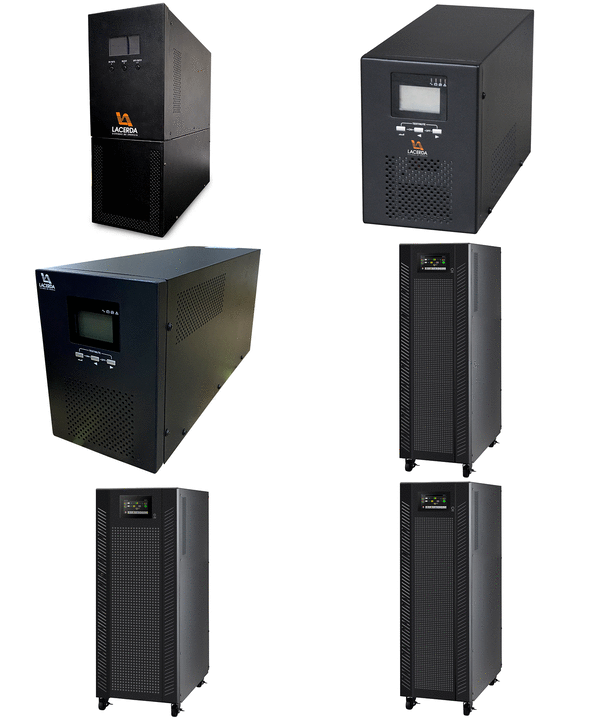
SINGLE -PHASE PROTOTYPE WITH INFINEON 1700V-JFETS
THREE-PHASE PROTOTYPE WITH INFINEON 1700V-JFETS
ON THE PERSPECTIVES OF WIDE-BAND GAP POWER DEVICES IN ELECTRONIC-BASED POWER CONVERSION FOR RENEWABLE SYSTEMS AUTHOR SAMUEL VASCONCELOS ARAÚJO
THESIS THE ACADEMIC DEGREE OF DOKTOR DER INGENIEUR-WISSENSHAFTEN (DR-ING).FACULTY OF ELECTRICAL ENGINEERING COMPUTER SCIENCES OF THE UNIVERSITY OF KASSEL GERMANY
FOREWORD
Power Electronics is taking an increasingly important role in our dailt lives, as it is the keystone not only to be efficient , but also cost effective and reliable use of electric energy in all possible fields of aplication;ranging from power supply from renewable energy sources to industry,IT and transportation.
The first revolution in this field of technology came in the 1960 with the viability of switched-mode power conversion ,owning to the emergence of BJTs operating at higher speeds.The development of MOSFETs and later IGBTs provided a futher step in the direction towards higher frequency and power levels.
The advent of power device based on silicon carbide (SiC) and gallium nitride (GAn) is curently pointing in the direction of a second revolution,whwre several paradigms concernig the design and performance of power conversion stages will be broken.
FULL THESIS
http://www.uni-kassel.de/upress/online/frei/978-3-86219-486-5.volltext.frei.pdf
Dr.Ing. SAMUEL VASCONCELOS ARAÚJO (FACULTY OF ELECTRICAL ENGINEERING COMPUTER SCIENCES OF THE UNIVERSITY OF KASSEL GERMANY) ,GRADUATION STUDENT IN THE FEDERAL UNIVERSITY OF CEARA (UFC-2005)
BRASIL WORKING IN THE GEPEC LABORATORY.
No Blog Eletrônica de Potência você encontrará informações sobre teses,artigos,seminarios,congressos,tecnologias,cursos,sobre eletrônica potência. “TEMOS O DESTINO QUE MERECEMOS. O NOSSO DESTINO ESTA DE ACORDO COM OS NOSSOS MERITOS” ALBERT EINSTEIN. Imagination is more important than knowledge, for knowledge is limited while imagination embraces the entire world. EL FUTURO SE CONSTRUYE HOY,EL SUCESSO NO ES FRUTO DE LA CASUALIDAD,SE HUMILDE ,APRENDE SIEMPRE CADA DIA.
AUTOR DO BLOG ENG.ARMANDO CAVERO MIRANDA SÃO PAULO BRASIL

.gif)
“GRAÇAS A DEUS PELA VIDA,PELA MINHA FAMÍLIA,PELO TRABALHO.PELO PÃO DE CADA DIA,POR NOS PROTEGER DO MAL”
“SE SEUS PROJETOS FOREM PARA UM ANO,SEMEIE O GRÂO.SE FOREM PARA DEZ ANOS,PLANTE UMA ÁRVORE.SE FOREM PARA CEM ANOS,EDUQUE O POVO”


https://picasion.com/


terça-feira, 25 de novembro de 2014
segunda-feira, 24 de novembro de 2014
EMC: A mapping for the Compact Muon Solenoid CMS experiment Fernando José González Arteche TESIS DOCTORAL UNIVERSIDAD DE OVIEDO Departamento de Ingeniería Eléctrica, Electrónica, de Computadores y Sistemas
EMC: A mapping for the Compact Muon Solenoid CMS experiment
Fernando José González Arteche
TESIS DOCTORAL UNIVERSIDAD DE OVIEDO
Departamento de Ingeniería Eléctrica, Electrónica, de Computadores
y Sistemas
ABSTRACT
Introduction The Compact Muon Solenoid (CMS) is one of the four high-energy physics experiments under construction at CERN for the Large Hadron Collider (LHC) accelerator. The dimensions of the CMS detector are about 30 meters long and 25-meter diameter, with a total weight of around 13000 tons. The CMS detector is divided in five sub-systems located at different layers of the structure. Each sub-system has distinct objectives and processes different signal and energy levels. In general, high-energy physics (HEP) experiments identify particle interactions and measure their energy using sensitive detection devices such as silicon and pixel detectors, wire chambers, scintillators and optical devices. In the CMS experiment, the detected electrical signal is amplified and processed by the front-end electronics (FEE), which communicate, via optical links, with the acquisition system located 120 meters away from the detector. The read-out electronics of the CMS experiment are designed to process signals of a few mV digitizing them synchronously at 40 MHz. Part of this electronics is located inside of a harsh environment with particle radiation and a DC magnetic field of 4 Tesla.
FULL THESIS
https://copy.com/jpKjlUr08vtbguho
domingo, 23 de novembro de 2014
PROJETO RETIFICADOR MONOFASICO

ARCHIVO EN PDF
https://copy.com/cERrgAOLsMUbtVYO
LINK1-ARCHIVO MATHCAD
https://copy.com/chjXIXUqf0APA1PG
LINK2-ARCHIVO-MATHCAD
https://copy.com/zfGFYJFmTI9edQXu
Assinar:
Postagens (Atom)


