AUTOR DO BLOG ENG.ARMANDO CAVERO MIRANDA SÃO PAULO BRASIL

"OBRIGADO DEUS PELA VIDA,PELA MINHA FAMILIA,PELO TRABALHO,PELO PÃO DE CADA DIA,PROTEGENOS DO MAL"

"OBRIGADO DEUS PELA VIDA,PELA MINHA FAMILIA,PELO TRABALHO,PELO PÃO DE CADA DIA,PROTEGENOS  DO MAL"

“SE SEUS PROJETOS FOREM PARA UM ANO,SEMEIE O GRÂO.SE FOREM PARA DEZ ANOS,PLANTE UMA ÁRVORE.SE FOREM PARA CEM ANOS,EDUQUE O POVO.”

“Sixty years ago I knew everything; now I know nothing; education is a progressive discovery of our own ignorance. Will Durant”

https://picasion.com/

domingo, 30 de junho de 2024

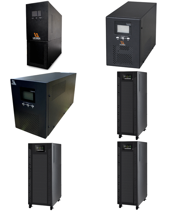
NO-BREAK PARA APLICAÇÕES RESIDENCIAIS, COMERCIAIS E INDUSTRIAIS DE 5kW COM INTERFACE PARA PAINEL SOLAR Carlos H. G. Treviso, Aziz E. Demian Jr., André L. B. Ferreira -Universidade Estadual de Londrina - Londrina - PR -BRASIL


NO-BREAK PARA APLICAÇÕES RESIDENCIAIS, COMERCIAIS E INDUSTRIAIS DE 5kW COM INTERFACE PARA PAINEL SOLAR 
Carlos H. G. Treviso, Aziz E. Demian Jr., André L. B. Ferreira Universidade Estadual de Londrina - UEL CEP 86055-900, C.P. 6001, Londrina - PR -BRASIL 

 Resumo – Este artigo traz um projeto completo de um No-Break de 5kW de saída, para aplicações residenciais, comerciais e industriais, sendo uma importante contribuição para o meio acadêmico e comercial. Permite ainda a utilização de painéis solares, podendo tornar a carga em questão menos dependente da rede elétrica, além da utilização da energia limpa. Para tanto foi implementado um protótipo em campo, com banco de baterias de 48V (24 baterias de 12V/7,2A), com estimativa de autonomia de 25 minutos para carga máxima. 

 RESIDENTIAL, COMMERCIAL AND INDUSTRIAL APPLICATIONS FOR A 5kW UPS UNIT WITH INTERFACE FOR SOLAR PANNEL COUPLING

 Abstract – This article presents the complete project for a 5kW UPS unit devised, for residential, commercial and industrial applications that is an important contributing for the academic and commercial environment. It allows the use of solar panels, that can make the load less dependent on electric system and the use of clean energy. For this was implemented a prototype in field, with batteries bank of 48V (batteries of 12V/7,2A), with 25 minute estimate autonomy for maximum load.

VIEW FULL TEXT:

quinta-feira, 20 de junho de 2024

Power Line Noise Suppression using N-path Notch Filter in ECG Signal Acquisition-Doctoral Thesis Shibaura Institute of Technology-Author: Khilda AFIFAH


POWER LINE NOISE SUPPRESSION USING N-PATH NOTCH FILTER IN ECG SIGNAL ACQUISITION Author: Khilda AFIFAH Supervisor: Prof. Nicodimus RETDIAN 

A thesis submitted in fulfillment of the requirements for the award of the degree of Doctor of Engineering Shibaura Institute of Technology 2020/September

Abstract
 POWER LINE NOISE SUPPRESSION USING N-PATH NOTCH FILTER IN ECG SIGNAL ACQUISITION by Khilda AFIFAH

 Bio-sensing activities such as electrocardiogram (ECG) and electroencephalography (EEG) are challenging to obtain high-quality electrical signals because biomedical signals have small amplitude and low frequency. When performing a biomedical signal acquisition, common-mode noise such as power line interference appears near the desired biomedical signal. It has made a problem when the power line interference has amplitude higher than the primary signal. Common-mode noise reduction has been recognized as important research. The driven right leg (DRL) circuit was significant and effective to suppress commonmode noise. However, in the actual ECG measurements using DRL circuit, sometimes noise still appears at the output and mismatching in the electrode impedance makes an impact to convert common-mode noise into a differential input voltage. The body in DRL circuit is expressed as a single node and cannot be used to simulate the effect of the electrode impedance mismatch. Therefore, a new body model is needed to be able to analyze the effect of electrode impedance mismatch and other problem with common body model. 
The proposed DRL circuit is an improved circuit from common DRL circuit. The first improved DRL circuit, biomedical signal is expressed by current source in parallel with electrode impedance. The simulation results of improved circuit show mismatch between right and left electrode impedance makes noise appears at the output signal. The common human body from DRL circuit represented skin-electrode impedance as a single node. The second improved circuit, the skin-electrode impedance is expressed by resistance and stray capacitance are on each electrode. The simulation results of this improved circuit show the proposed circuit achieved smaller noise when stray capacitance in the arm and right leg are the same. Combination between proposed human body model and DRL circuit achieved output of the circuit is noise appear in the output signal. Therefore, human body model with DRL circuit still need another filter to get high quality biomedical signal (noise free signal).

The other techniques to suppress common-mode noise have been proposed by using digital and analog notch filters. The technique to suppress common-mode noise used a digital notch filter, but it requires an analog front-end with a wide dynamic range since the noise contaminated input signal need to be converted to digital signal. The techniques with analog notch filter such as conventional Npath notch filters have disadvantage because these techniques require 3GΩ switches off-resistance and 18 paths to reach notch depth target. The problem to implement previous N-path notch filter is the difficulty in implementing switch with offresistance. On-chip implementation of the system is also a challenge in the realization of portable ECG devices because the notch filter has a large time constant in which requires large capacitance and high resistance. Two topologies of N-path notch filter with leak buffer circuit have been proposed. The proposed N-path notch filters are Topology 1 and Topology 2. Topology 1 and Topology 2 achieved notch depth of 62.4dB and 63dB in measurement results with sampling frequency 50Hz, even if the proposed circuits use less number of path and small of switches off-resistance. Topology 1 and Topology 2 are verified using artificial ECG signal with 2Hz which is contaminated by power line interference with frequency 50Hz or 60Hz. Experiment results show that the proposed circuit significantly reduces the power line noise.
VIEW FULL THESIS:


quinta-feira, 23 de maio de 2024

PSpice Simulation - Parametric Sweep

PSPICE SIMULATION - PARAMETRIC SWEEP ※ 

Parametric Sweep conducts simulation by changing element values ​​set as variables in the circuit. This has been covered in the previous DC sweep, and this is because Parametric Sweep can be implemented not only by sweeping variables arbitrarily set by the user, but also by changing the values ​​of used elements. 

 1. Circuit diagram


After writing, apply vcc and vee through the vcc element of place power, and give the name of the out node through place net alias. 

 One thing to note here is that the value of resistance R2 must be entered as {Rvar}. This means that it will have a value as a variable called Rvar. 

 Also, pay attention to the input terminal sign of LM324. After placing the element, you must press the V key to invert it up and down. 

 Now we need to set the value of the variable Rvar. 

The value of the variable uses the element that appears when you search for PARAM in the place part.


After placing the element, double-click on the element to modify its properties.


If you double-click the upper left corner of the table that appears, the property will change from horizontal alignment to vertical alignment.


Click New Row at the top left.
Enter Rvar corresponding to the variable name as the new property and 200 as the desired initial value. Click Apply to continue adding new rows, and click OK to finish. When finished, press OK. Place the mouse cursor on the added value of Rvar, right-click, and select display.


Select Name and Value from the properties that appear.


Press OK, right-click the open tab to save it, then right-click again to close it.


When you return to the circuit diagram, you can see that the initial values ​​of the variables have been set.

2. Simulation settings


Select AC Sweep/Noise. It varies from 10 to 100 kHz and has 100 points per section.


Check Parametric Sweep in Options on the left. 

 Since the value you want to change is a variable called Rvar set by the user, select Global Parameter and write Rvar in the name. The value is increased by 200 from 200 to 1k.


If you do not want to change the value linearly but want to change it to specific values, select Sweep type as Value list at the bottom instead of Linear and write the values. Values ​​can be separated by spaces or commas. ex) 5m, 10m, ... Once the setup is complete, place a dB scale voltage probe as in the previous AC sweep post.


3. Execution result

 If you run the simulation, you can get the following results.


You can see that the area of ​​the pass band is different depending on each resistance value. 

 Therefore, for analysis, let's find the area of ​​the pass band that is 3dB lower than the maximum value. Since it is analyzed using multiple results, it must be interpreted through the performance analysis discussed earlier. 

 When performing performance analysis using the methods discussed above, there are times when it does not execute due to errors. 

 Therefore, this time we will proceed with performance analysis in a slightly different way.

First, click the Perfromance analysis icon on the toolbar at the top of the simulation window.


Then, a new plot is created at the top, and you can confirm that it is selected through SEL>>.

 Select Trace > Add trace from the menu at the top of the simulation window.


First, select Bandwidth_Bandpass_3dB(1) from the functions on the right ,

 and then select V(out) from the variables on the left.


Then, you can check the size of the pass band according to the Rvar value.


Please keep in mind that performance analysis is used when interpreting multiple results.