AUTOR DO BLOG ENG.ARMANDO CAVERO MIRANDA SÃO PAULO BRASIL

"OBRIGADO DEUS PELA VIDA,PELA MINHA FAMILIA,PELO TRABALHO,PELO PÃO DE CADA DIA,PROTEGENOS DO MAL"

"OBRIGADO DEUS PELA VIDA,PELA MINHA FAMILIA,PELO TRABALHO,PELO PÃO DE CADA DIA,PROTEGENOS  DO MAL"

“SE SEUS PROJETOS FOREM PARA UM ANO,SEMEIE O GRÂO.SE FOREM PARA DEZ ANOS,PLANTE UMA ÁRVORE.SE FOREM PARA CEM ANOS,EDUQUE O POVO.”

“Sixty years ago I knew everything; now I know nothing; education is a progressive discovery of our own ignorance. Will Durant”

domingo, 16 de agosto de 2020

Updating and Customizing an industrial UPS HMI-A Master's Thesis Submitted to the Faculty of the Escola Tècnica d'Enginyeria de Telecomunicació de Barcelona Universitat Politècnica de Catalunya by Ali Ahmadi


 Abstract 
Uninterruptable Power Supply or UPS is one of the key parts of industries nowadays. Importance of it has risen because of the increasing demand for more stable power supply for Electronics and Electrical systems each year, especially in the field of IT and Data Servers. During these years, with improving Electrical products, Human Machine Interface became part of most electrical products and UPS is no exception. These days, UPS has a graphical display which according to the application of UPS, its design and abilities is different. HMI design for UPS has challenges, as instance: design according to the application, efficiency of design, preventing bugs, graphical design and etc. During this project, our plan is designing a new generation of Salicru HMI with the capability of adopting with old version Industrial UPS which manufactured by partner companies and also this HMI use for Salicru new generation UPS, Cube 4.

quinta-feira, 13 de agosto de 2020

Optimal Design Method of the LLC resonant converter using the hybrid current balancing circuit for LED lighting -Author Jin-Gu Kim Department of Electrical & Medical Convergent Engineering Graduate School, Kangwon National University South Korea.


Optimal Design Method of the LLC resonant converter using the hybrid current balancing circuit for LED lighting  Author Jin-Gu Kim

 Department of Electrical & Medical Convergent Engineering Graduate School, Kangwon National University South Korea.

Abstract 

In this thesis, a novel hybrid current balancing circuit and an optimum design of LLC resonant converter for driving a current balancing circuit are proposed. 

First of all, the hybrid current balancing circuit was proposed for compensating current deviation among LED strings. LEDs have been widely used in lighting, automobiles, and airplanes owing to their excellent light output characteristics and long lifespan. Though LEDs are manufactured under the same process, variations in impurity concentrations cause electrical deviation among LEDs. This electrical deviation results in current unbalance of LED strings. The resulting current unbalance does not only reduce the life time of the LED but also cause non-uniform luminance of LEDs connected in parallel. The LED driving circuit is researched to solve the above problems. In this thesis, a novel hybrid current balancing circuit with a Y-type current balancing transformer and a voltage doubler rectifier circuit was proposed for the compensation of 6 LED strings with a simple structure.

 Secondly, the Optimal design method of LLC resonant converter for driving hybrid current balancing circuit was proposed. The difference between the proposed optimal design method of LLC resonant converter and conventional design method can be divided into three categories.

 First of all, when designing transformer with leakage inductance(Lr ) and magnetizing inductance(Lm), unwanted leakage inductance of secondary side (Lr2) which cause error in the process of measuring the leakage inductance (Lr ) with instrument occurs. This design error could be reduced by taking into account the leakage inductance of secondary side(Lr2). 

Secondly, in general, the voltage gain characteristic curve is applied to design LLC resonant converter. in this thesis, the current gain characteristic curve was applied to the design process which is suitable for LED that is non-linear load and necessary to be controlled to a constant current. 

Lastly, the equivalent circuit of LED was applied to the design process. Normally, a resistive load which has linear load characteristic is used for designing the LLC resonant converter. However, in this thesis, the equivalent circuit of LED which includes a voltage source, a resistor and a diode could be obtained by using the linear approximation method. This circuit was then applied to the design process for reducing design error. 

Experimental results are presented to verify the performance of the proposed hybrid current balancing circuit and the optimal design method of the LLC resonant converter. The LED maximum current error rate which was 19.57% was reduced to 4.5% by Y-type current balancing transformer. Also, the validity of the proposed optimal design method of the LLC resonant converter was verified by comparing it with the conventional design method. 
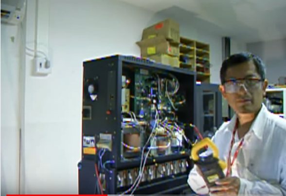
An 150W prototype was implemented and used for the performance verification of the hybrid current balancing circuit and the LLC resonant converter.

LINK: http://www.mediafire.com/file/sfzdhsuo3y91zod/file

terça-feira, 11 de agosto de 2020

Master's Thesis Design, Control, and Implementation of High Frequency LLC Resonant Converter-Author- Hwa-Pyeong Park Department of Electrical and Computer Engineering -ULSANG NATIONAL INSTITUTE OF SCIENCE AND TECHNOLOGY


 Master's Thesis
 Design, Control, and Implementation of High Frequency LLC Resonant Converter Hwa-Pyeong Park Department of Electrical and Computer Engineering 

 Abstract
 A high switching frequency operation has been introduced with much interest in research and industrial areas to improve the power density of power converters. However, its implementation is difficult for an elaborate switch mode power supply which has high efficiency and stable operation. In this paper, a power stage and a feedback controller design will be considered for proper operation, stability, and high power conversion efficiency of the high frequency LLC resonant converter. The power density can be improved by adopting high switching frequency which allows small sized passive components. At the high switching frequency, the size reduction of the passive components such as transformer, and output capacitor will be estimated to obtain the high power density design. In addition, the design method of the magnetizing inductance design method will be derived to achieve the zero voltage switching (ZVS) at the high switching frequency operation. In aspect of frequency domain, the smaller output capacitor which has small capacitance and low effective series resistance (ESR) changes the small-signal behavior of the converter’s power stage. It can make the converter unstable by increasing the crossover frequency in the loop gain of the smallsignal model. The effect of the smaller output capacitance should be analyzed for stability analysis using a proper small-signal model of the LLC resonant converter. Therefore, the proper design methods of the feedback compensator are derived to obtain sufficient phase margin in the bode plot of the converter’s loop gain for its stable operation. The design considerations of the power stage and the feedback loop will be verified with the performance comparison of 100 kHz and 500 kHz switching frequency LLC resonant converters. Since the switching performance of state-of-art power switches has been improved, the power converter can operate over a 1 MHz switching frequency. In this paper, GaN E-HEMTs are used to achieve the high switching frequency operation due to its small channel resistance and small output capacitance. However, the GaN E-HEMTs also have different switching operation characteristics to other conventional silicon-based MOSFETs. Therefore, the high speed switching characteristics of the GaN E-HEMT should be analyzed to obtain proper operation for a half-bridge type LLC resonant converter using a boostrap gate drive circuit. Moreover, a soft start algorithm for the high switching frequency is analyzed to suppress inrush currents at the cold start operation of the converter. All the design considerations using the GaN E-HEMT are verified with a 240 W prototype LLC resonant converter operating at 1 MHz switching frequency.

sábado, 8 de agosto de 2020

Méthodologie de conception numérique d’un module de puissance dédié à l’automobile en vue de l’optimisation des surtensions, des pertes et des émissions conduites Hocine Dao--Thèse de doctorat de l'Université Paris-Saclay préparée à L’École Normale Supérieure de Cachan (École normale supérieure Paris-Saclay)-


Méthodologie de conception numérique d’un module de puissance dédié à l’automobile en vue de l’optimisation des surtensions, des pertes et des émissions conduites 
Hocine Dao
Thèse de doctorat de l'Université Paris-Saclay préparée à L’École Normale Supérieure de Cachan (École normale supérieure Paris-Saclay)

 Résumé : 
Le véhicule électrique (VE) s'inscrit actuellement dans un contexte industriel fortement corrélé aux contraintes environnementales. Un tel contexte où la minimisation des coûts est également vitale impose par conséquent des contraintes de développement et de réalisation. Les modules de puissance constituent un coût conséquent dans un système de conversion pour l'automobile. Nous nous plaçons dans le contexte des modules de puissance à IGBT en technologie silicium qui assurent les fonctions de conversion d’énergie (AC/DC ou DC/AC) pour des applications moyennes et fortes puissances. L’un des points les plus limitant de ces modules est l’aspect inductif de la maille de commutation. L’intégration de condensateurs de découplage (Ceq) au sein du module permet de réduire les effets des inductances parasites car ils offrent un chemin à basse impédance au courant commuté et augmentent la vitesse de commutation du composant. C’est cette solution que nous avons étudiée. Le but est de démontrer la faisabilité d’une telle solution couplée avec le choix optimal de la résistance de grille (Rg) des puces IGBT. Nous avons établi des règles de conception permettant la construction de modèles circuit d’un bras d’onduleur permettant l’intégration de fonction de découplage. Ce dernier nous a permis dans un premier temps de réduire les surtensions aux bornes des composants mais les pertes par commutation n’ont pas pu être améliorées significativement en comparaison à un module conventionnel. La démarche suivie pour aller plus loin a consisté à chercher un compromis entre les valeurs des condensateurs distribués dans le module et le choix des résistances de grille des puces IGBT. L’optimisation par algorithmes génétiques est la solution qui a été trouvée pour contourner les problèmes bloquants et améliorer significativement les performances du module.

Vieillissement accéléré de modules de puissance de type MOSFET SiC et IGBT Si basé sur l'analyse de profils de mission d'onduleurs photovoltaïques. Mouhannad Dbeiss--Institut Polytechnique de Grenoble

Vieillissement accéléré de modules de puissance de type MOSFET SiC et IGBT Si basé sur l'analyse de profils de mission d'onduleurs photovoltaïques
Autor: Mouhannad Dbeiss 
 Thèse dirigée par Yvan AVENAS, Maître de Conférences HdR, Institut Polytechnique de Grenoble préparée au sein du CEA/INES dans l'École Doctorale Electronique, Electrotechnique, Automatique, Traitement du Signal (EEATS)

Abstract
In the case of photovoltaic installations, the DC/AC inverter has the highest failure rate, and the anticipation of its breakdowns is still difficult, while few studies have been done on the reliability of this type of inverter. The aim of this PhD is to propose tools and methods to study the ageing of power modules in this type of application, by focusing on ageing phenomena related to thermo-mechanical aspects.
As a general rule, the accelerated ageing of power modules is carried out under aggravated conditions of current (Active Cycling) or temperature (Passive Cycling) in order to accelerate the ageing process. Unfortunately, when applying this type of accelerated ageing tests, some failure mechanisms that do not occur in the real application could be observed, while inversely, other mechanisms that usually occur could not be recreated.
The first part of the PhD focuses on the implementation of an accelerated ageing method of the semiconductor devices inside photovoltaic inverters. This is accomplished by analyzing the mission profiles of the inverter’s output current and ambient temperature, extracted over several years from photovoltaic power plants located in the south of France. These profiles are used to study photovoltaic current dynamics, and are introduced into numerical models to estimate losses and junction temperature variations of semiconductors used in inverters, using the cycle counting algorithm “Rainflow”.
This method is then performed in two experimental test benches. In the first one, the devices under test are IGBT modules, where the accelerated ageing profile designed is implemented using the opposition method. Moreover, an in-situ setup for monitoring ageing indicators (thermal impedance and dynamic resistance) is also proposed and evaluated. The second bench is devoted to study the ageing of SiC MOSFET power modules. The accelerated ageing test is carried out under the same conditions as for the IGBT modules with more monitored electrical indicators, but this time by disconnecting the semiconductor devices from the inverter. The results obtained allowed to determine several potential ageing indicators of IGBTs and SiC MOSFETs used in a photovoltaic inverter.