AUTOR DO BLOG ENG.ARMANDO CAVERO MIRANDA SÃO PAULO BRASIL

"OBRIGADO DEUS PELA VIDA,PELA MINHA FAMILIA,PELO TRABALHO,PELO PÃO DE CADA DIA,PROTEGENOS DO MAL"

"OBRIGADO DEUS PELA VIDA,PELA MINHA FAMILIA,PELO TRABALHO,PELO PÃO DE CADA DIA,PROTEGENOS  DO MAL"

“SE SEUS PROJETOS FOREM PARA UM ANO,SEMEIE O GRÂO.SE FOREM PARA DEZ ANOS,PLANTE UMA ÁRVORE.SE FOREM PARA CEM ANOS,EDUQUE O POVO.”

“Sixty years ago I knew everything; now I know nothing; education is a progressive discovery of our own ignorance. Will Durant”

https://picasion.com/

terça-feira, 23 de julho de 2024

전압 직렬보상 방식 디지털 제어 교류 저전압보상기 정 강 률* Digital-Controlled AC Low-Voltage Compensator with Voltage Series Compensation Method Gang-Youl Jeong*


전압 직렬보상 방식 디지털 제어 교류 저전압보상기 정 강 률* Digital-Controlled AC Low-Voltage Compensator with Voltage Series Compensation Method Gang-Youl Jeong* Journal of KIIT. Vol. 21, No. 12, pp. 87-98, Dec. 31, 2023. pISSN 1598-8619, eISSN 2093-7571 87 

 Abstract 

This paper presents the digital-controlled AC low-voltage compensator with voltage series compensation method. The proposed AC low-voltage compensator compensates for the magnitude of the AC load input voltage, which is the final output voltage, with the voltage series compensation method using a power circuit topology consisting of a pulse-width modulation(PWM) AC-AC power converter and a compensating transformer. To this end, the proposed low-voltage compensator simply feeds back the magnitude of AC load input voltage through a circuit consisting of a current-type voltage transformer, a diode full-bridge rectifier, and a resistor/capacitor. Additionally, using a micom, it converts the feedback voltage to a digital value through A/D conversion and easily controls the entire system. This paper first briefly describes the operating principle of the power converter applied to the proposed low-voltage compensator and explains the control method of low-voltage compensation and the feedback method of final output voltage. Then, the driving method of the bidirectional power semiconductor switch of power converter is explained, and the implementation feasibility and good operating characteristics of the proposed low-voltage compensator are validated through the experimental results of the prototype.

단일단 교류 전력변환기를 이용한 자동 교류 전압조정기-Automatic AC Voltage Regulator using the Single-Stage AC Power Converter Gang-Youl Jeong*


단일단 교류 전력변환기를 이용한 자동 교류 전압조정기 정 강 률* Automatic AC Voltage Regulator using the Single-Stage AC Power Converter Gang-Youl Jeong* Journal of KIIT. Vol. 20, No. 11, pp. 73-83, Nov. 30, 2022. pISSN 1598-8619, eISSN 2093-7571 73 

 Abstract 

This paper presents the automatic AC voltage regulator using the single-stage AC power converter. The proposed automatic AC voltage regulator uses a pulse-width modulation(PWM) type non-isolated single-stage step-up/down AC power converter to control and maintain the level of AC voltage on the output-side to a desired level. Since the proposed voltage regulator controls the magnitude of output voltage by using only the average of the scaling values of the output voltage fed back by a simple voltage feedback circuit without phase synchronization, the control method of output voltage is simple. Thus, the proposed voltage easily controls the entire system using a single-chip microcontroller. In this paper, first, the operating principle of the power converter of proposed voltage regulator is briefly explained, and then the feedback and control method of output voltage are described. The feasibility and operating characteristics of proposed voltage regulator are verified through the experimental results of prototype. The proposed voltage regulator can control and maintain the output-side AC voltage to a desired level by performing the step-up/down control operation accurately, and shows a fast dynamic response characteristic.

domingo, 30 de junho de 2024

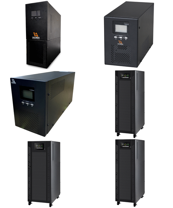
NO-BREAK PARA APLICAÇÕES RESIDENCIAIS, COMERCIAIS E INDUSTRIAIS DE 5kW COM INTERFACE PARA PAINEL SOLAR Carlos H. G. Treviso, Aziz E. Demian Jr., André L. B. Ferreira -Universidade Estadual de Londrina - Londrina - PR -BRASIL


NO-BREAK PARA APLICAÇÕES RESIDENCIAIS, COMERCIAIS E INDUSTRIAIS DE 5kW COM INTERFACE PARA PAINEL SOLAR 
Carlos H. G. Treviso, Aziz E. Demian Jr., André L. B. Ferreira Universidade Estadual de Londrina - UEL CEP 86055-900, C.P. 6001, Londrina - PR -BRASIL 

 Resumo – Este artigo traz um projeto completo de um No-Break de 5kW de saída, para aplicações residenciais, comerciais e industriais, sendo uma importante contribuição para o meio acadêmico e comercial. Permite ainda a utilização de painéis solares, podendo tornar a carga em questão menos dependente da rede elétrica, além da utilização da energia limpa. Para tanto foi implementado um protótipo em campo, com banco de baterias de 48V (24 baterias de 12V/7,2A), com estimativa de autonomia de 25 minutos para carga máxima. 

 RESIDENTIAL, COMMERCIAL AND INDUSTRIAL APPLICATIONS FOR A 5kW UPS UNIT WITH INTERFACE FOR SOLAR PANNEL COUPLING

 Abstract – This article presents the complete project for a 5kW UPS unit devised, for residential, commercial and industrial applications that is an important contributing for the academic and commercial environment. It allows the use of solar panels, that can make the load less dependent on electric system and the use of clean energy. For this was implemented a prototype in field, with batteries bank of 48V (batteries of 12V/7,2A), with 25 minute estimate autonomy for maximum load.

VIEW FULL TEXT:

quinta-feira, 20 de junho de 2024

Power Line Noise Suppression using N-path Notch Filter in ECG Signal Acquisition-Doctoral Thesis Shibaura Institute of Technology-Author: Khilda AFIFAH


POWER LINE NOISE SUPPRESSION USING N-PATH NOTCH FILTER IN ECG SIGNAL ACQUISITION Author: Khilda AFIFAH Supervisor: Prof. Nicodimus RETDIAN 

A thesis submitted in fulfillment of the requirements for the award of the degree of Doctor of Engineering Shibaura Institute of Technology 2020/September

Abstract
 POWER LINE NOISE SUPPRESSION USING N-PATH NOTCH FILTER IN ECG SIGNAL ACQUISITION by Khilda AFIFAH

 Bio-sensing activities such as electrocardiogram (ECG) and electroencephalography (EEG) are challenging to obtain high-quality electrical signals because biomedical signals have small amplitude and low frequency. When performing a biomedical signal acquisition, common-mode noise such as power line interference appears near the desired biomedical signal. It has made a problem when the power line interference has amplitude higher than the primary signal. Common-mode noise reduction has been recognized as important research. The driven right leg (DRL) circuit was significant and effective to suppress commonmode noise. However, in the actual ECG measurements using DRL circuit, sometimes noise still appears at the output and mismatching in the electrode impedance makes an impact to convert common-mode noise into a differential input voltage. The body in DRL circuit is expressed as a single node and cannot be used to simulate the effect of the electrode impedance mismatch. Therefore, a new body model is needed to be able to analyze the effect of electrode impedance mismatch and other problem with common body model. 
The proposed DRL circuit is an improved circuit from common DRL circuit. The first improved DRL circuit, biomedical signal is expressed by current source in parallel with electrode impedance. The simulation results of improved circuit show mismatch between right and left electrode impedance makes noise appears at the output signal. The common human body from DRL circuit represented skin-electrode impedance as a single node. The second improved circuit, the skin-electrode impedance is expressed by resistance and stray capacitance are on each electrode. The simulation results of this improved circuit show the proposed circuit achieved smaller noise when stray capacitance in the arm and right leg are the same. Combination between proposed human body model and DRL circuit achieved output of the circuit is noise appear in the output signal. Therefore, human body model with DRL circuit still need another filter to get high quality biomedical signal (noise free signal).

The other techniques to suppress common-mode noise have been proposed by using digital and analog notch filters. The technique to suppress common-mode noise used a digital notch filter, but it requires an analog front-end with a wide dynamic range since the noise contaminated input signal need to be converted to digital signal. The techniques with analog notch filter such as conventional Npath notch filters have disadvantage because these techniques require 3GΩ switches off-resistance and 18 paths to reach notch depth target. The problem to implement previous N-path notch filter is the difficulty in implementing switch with offresistance. On-chip implementation of the system is also a challenge in the realization of portable ECG devices because the notch filter has a large time constant in which requires large capacitance and high resistance. Two topologies of N-path notch filter with leak buffer circuit have been proposed. The proposed N-path notch filters are Topology 1 and Topology 2. Topology 1 and Topology 2 achieved notch depth of 62.4dB and 63dB in measurement results with sampling frequency 50Hz, even if the proposed circuits use less number of path and small of switches off-resistance. Topology 1 and Topology 2 are verified using artificial ECG signal with 2Hz which is contaminated by power line interference with frequency 50Hz or 60Hz. Experiment results show that the proposed circuit significantly reduces the power line noise.
VIEW FULL THESIS: