


quarta-feira, 28 de dezembro de 2022
sábado, 3 de dezembro de 2022
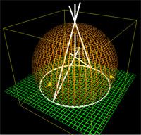
Self-powered Sensor Monitoring System in Industrial Internet of Things using Off-resonance Piezoelectric Energy Harvesting Techniques by Jae Yong Cho -Dissertation for the degree of Doctor of Philosophy-Graduate School of Hanyang University-


Dissertation for the degree of Doctor of Philosophy Self-powered Sensor Monitoring System in Industrial Internet of Things using Off-resonance Piezoelectric Energy Harvesting Techniques
by Jae Yong Cho
Graduate School of Hanyang University
February 2019
Department of Electrical Engineering
Graduate School of Hanyang University
ABSTRACT
The main keyword in the era of the fourth industrial revolution is IIoT (Industrial
Internet of Things) that enables the interactive network between devices, vehicles, home
appliances, and other items embedded with electronics, software, sensors, actuators and etc.
To realize IIoT world, there are key technologies; sensors, microcontroller, connectivity,
and energy management. Especially, in terms of energy management, many researches
have been carried out about self-powering, a battery-less device from energy harvesting.
At the center, there is piezoelectric energy harvesting technology, which converts
mechanical energy into electrical energy. Lots of researches about piezoelectric energy
harvesting have been carried about because piezoelectric material has relatively high power
density and is easily applicable to various infrastructures like road, building, and factory
close to our daily lives. Ultimately, the goal of this technology is heading for energy saving
and simple installation of sensors used for monitoring structural condition without
inconveniences such as the replacement of the batteries and the complexity of the cables.
In this dissertation, the research about design and fabrication of off-resonance type
piezoelectric energy harvesting systems for IIoT sensor was discussed. Because the actual
frequency environment in a real field is not geared to resonant frequencies, previous
piezoelectric energy harvesting systems were difficult to harvest ambient energy efficiently.
We developed the techniques for harvesting energy efficiently through new structures of
off-resonance piezoelectric energy harvesters according to various frequency environment.
As the final step, the demonstration study was conducted to illustrate IIoT platform as V2I
(Vehicle to Infrastructure) system from the piezoelectric energy harvesting techniques. The
developed harvester was fabricated and installed on the highway (Yeoju-si, Gyeonggi-do,
South Korea). As a result, self-powered temperature sensor monitoring system was
constructed using the energy harvester to be able to operate wireless temperature sensor
(eZ430-RF2500, Texas Instruments, USA) without battery. Finally, the system was
established to inform a driver of the freezing condition on the road in advance as V2I
system.
First, the design and fabrication of the resonance dependent type energy harvester
were conducted. We have developed the piezoelectric energy harvester using wind that is
dependent on the resonant frequency, which is a key component of piezoelectric power
generation. The experiment result showed that the difference in power generation
characteristics when and when not at resonant frequencies makes difficult for the energy
harvester to be applied to actual industrial environments where frequencies vary. Finally, it
is essential to develop energy harvesters considering these diverse frequency environments.
Second, the studies of energy harvesters optimized for different types of frequency
environments in industries were conducted. The frequency environment was divided in four
conditions (single frequency, multi frequency, random frequency, and intermittent
frequency). For single, multi and random frequency conditions, a magneto-mechanical
system was applied as the method of harvesting more energy utilizing magnetic forces. For
an intermittent condition, system design was conducted as the method to overcome the offresonance
region. In single frequency environment, conveyor belts within a smart factory
were presented as an experimental environment and the study was conducted to overcome
an environment using magnets on the core belt that is much lower than the resonant
frequencies of a typical piezoelectric device. In multi frequency environment, water pipes
located in plants or buildings were presented as an experimental environment, and to
harvest more energy, a hybrid system using piezoelectric energy harvester and
electromagnetic energy harvester was studied. In a random frequency environment, the
railway was proposed as experimental condition and the magnetic pendulum energy
harvester utilizing inertial moments was developed. The energy harvester for the
intermittent frequency environment was studied, taking into account the wireless switch
that is sometimes pressed by humans as one of the intermittent frequency environments.
Third, the research was carried out on the energy harvesting circuit, which is essential
for applying the energy harvester to the actual IIoT environment. Preferentially, equivalent
circuit modeling of piezoelectricity and impedance matching study was conducted to
deliver maximum power. The DC-DC converter study was also conducted to convert high
voltage of the piezoelectricity into low voltage so that actual sensor applications can be
self-driven by the energy harvester. Additionally, the research was conducted to create the
desired output voltage, and finally to establish the wireless communication interface.
VIEW FULL THESIS: https://www.mediafire.com/file/41mjvvokgymxczk/Self-powered+Sensor+Monitoring+System+in+Industrial+Internet+of+Things+using+Off-resonance.pdf/file
sexta-feira, 2 de dezembro de 2022
Projeto otimizado para minimização de perdas em um conversor bidirecional aplicado a sistemas autônomos de iluminação-Tese de doutorado- Autoria:Duarte, Renan Rodrigo-UNIVERSIDADE FEDERAL DE SANTA MARIA-BRASIL


RESUMO
O presente trabalho apresenta o desenvolvimento de um sistema autônomo de iluminação pública baseado em energia solar fotovolaica e diodos emissores de luz (LEDs). O sistema deve ser capaz de carregar um banco de baterias durante o dia através de um arranjo fotovoltaico e suprir uma carga LED durante a noite. Um conversor bidirecional com transistores de nitreto de gálio (GaN) é utilizado de forma a obter uma estrutura com elevado rendimento e, com isso, otimizar o tamanho do banco de baterias e arranjo fotovoltaico para maximizar a autonomia do sistema ou reduzir os custos de produção, dependendo dos objetivos da aplicação. Foi desenvolvida uma metodologia completa e otimizada para o projeto dos elementos deste sistema autônomo de iluminação. Esta metodologia baseia-se em um algoritmo de busca discreta que avalia um conjunto de componentes disponíveis comercialmente para determinar a melhor combinação de componentes e o melhor ponto de operação do circuito, de modo a minimizar as perdas de energia ao longo do período de operação do sistema. Neste documento é apresentada, inicialmente, uma revisão bibliográfica de aspectos teóricos relacionados aos sistemas autônomos de iluminação, como fonte fotovoltaica, baterias, carga LED, topologias de conversores e soluções comerciais disponíveis. Uma revisão sobre interruptores GaN também é apresentada, abrangendo seu histórico, princípio de funcionamento, características e estado da arte da tecnologia em termos de dispositivos comerciais. Para validar experimentalmente a topologia proposta, um protótipo de 100 W com frequência de comutação arbitrária foi desenvolvido e avaliado. No modo carregador de bateria, o circuito opera em 250 kHz e apresenta eficiências maiores que 92% em toda a faixa de potência com um valor máximo de 97,3%. No modo driver de LED, a frequência de operação escolhida foi de 345 kHz e uma eficiência máxima de 95,8% foi obtida. Para a validação da metodologia de projeto proposta, quatro conversores com potências de 30 W em modo driver e 150 W em modo carregador foram implementados e testados em diferentes pontos de operação. Com isso, comprovou-se que, considerando um conjunto de componentes, a metodologia é capaz de determinar o melhor ponto de operação para maximizar o rendimento, e, considerando diferentes conjuntos de componentes, determinar o melhor em termos de redução da energia perdida, de forma a maximizar a autonomia do sistema.
VER TESE COMPLETA:
terça-feira, 22 de novembro de 2022
Doctoral Dissertation A Three-Phase SCVD Based Boost Inverter with Low Common Mode Voltage for Transformerless Photovoltaic Grid-Connected System Department of Electrical Engineering Graduate School, Chonnam National University BY Tran Tan Tai


This study deals with a new type of inverter called a three-phase SCVD based boost
inverter. The introduced structure is a combination of an SCVD network and the three-phase
bridge to restrict the common-mode voltage. Therefore, the introduced inverter can produce
a high output voltage from the low input voltage. The DC-bus voltage of the introduced
solution stands at twice of the input voltage. Moreover, the variation in common-mode
voltage can o be restricted within one-sixth of DC-bus voltage. Modeling, circuit analysis,
operating principles, and a comparison between the introduced SCVD based boost inverter
with the other VSIs are performed. To confirm the performance improvements of the
introduced SCVD based boost inverter, a preliminary prototype of the introduced SCVD
based boost inverter is built in the laboratory and the simulation studies based on PLECS
environment and experimental studies are performed. Besides that, a modified SCVD based
boost inverter is also introduced to step up the DC-bus voltage to triple of input voltage
instead of twice of input voltage like that in the proposed SCVD based boost inverter.
Furthermore, a common-mode voltage of the modified SCVD based boost inverter is
x
canceled through switching the four extra active-switches based on the Boolean logic
function. As a result, common-mode voltage is maintained as constant at the value of 0 V
during all time. Moreover, the voltage stress across additional semiconductor devices is
standing at one-third of DC-bus voltage. The simulation studies based on PLECS
environment prove the effectiveness of the modified SCVD based boost inverter. Finally, to
validate the performance, operating principle, and feasibility of the modified SCVD based
boost inverter, the experimental studies based on the laboratory prototype with a DSP
F280049C are carried out.
Doctoral Dissertation
A Three-Phase SCVD Based Boost Inverter with
Low Common Mode Voltage for Transformerless
Photovoltaic Grid-Connected System
Department of Electrical Engineering
Graduate School, Chonnam National University
BY Tran Tan Tai
(Abstract)
This study deals with a new type of inverter called a three-phase SCVD based boost
inverter. The introduced structure is a combination of an SCVD network and the three-phase
bridge to restrict the common-mode voltage. Therefore, the introduced inverter can produce
a high output voltage from the low input voltage. The DC-bus voltage of the introduced
solution stands at twice of the input voltage. Moreover, the variation in common-mode
voltage can o be restricted within one-sixth of DC-bus voltage. Modeling, circuit analysis,
operating principles, and a comparison between the introduced SCVD based boost inverter
with the other VSIs are performed. To confirm the performance improvements of the
introduced SCVD based boost inverter, a preliminary prototype of the introduced SCVD
based boost inverter is built in the laboratory and the simulation studies based on PLECS
environment and experimental studies are performed. Besides that, a modified SCVD based
boost inverter is also introduced to step up the DC-bus voltage to triple of input voltage
instead of twice of input voltage like that in the proposed SCVD based boost inverter.
Furthermore, a common-mode voltage of the modified SCVD based boost inverter is
canceled through switching the four extra active-switches based on the Boolean logic
function. As a result, common-mode voltage is maintained as constant at the value of 0 V
during all time. Moreover, the voltage stress across additional semiconductor devices is
standing at one-third of DC-bus voltage. The simulation studies based on PLECS
environment prove the effectiveness of the modified SCVD based boost inverter. Finally, to
validate the performance, operating principle, and feasibility of the modified SCVD based
boost inverter, the experimental studies based on the laboratory prototype with a DSP
F280049C are carried out.
VIEW FULL DOCTORAL DISSERTATION:
LINK ALTERNATIVO DOCTORAL DISSERTATION:
sexta-feira, 18 de novembro de 2022
GaN MOSFET를 이용한 유도전동기 구동용 고효율 인버터에 관한 연구 = A Study on the high efficiency inverter for driving an induction motor using GaN MOSFET by Park, Sang-Yong- Dept. of Electronic Engineering The Graduate School Hanyang University


A Study on the High Efficiency Inverter for Driving an
Induction Motor using GaN MOSFET
Park, Sang-yong
Dept. of Electronic Engineering
The Graduate School
Hanyang University
ABSTRACT
It was proved in this paper that the efficiency of the inverter using GaN
MOSFET ,which is regarded as a next generation power semiconductor,
was much improved comparing the efficiency to the counterpart using the
conventional Si MOSFET. Comparing the characteristics of GaN MOSFET
to those of Si MOSFET, GaN MOSFET shows very low on resistance and
very fast switching speed due to the high breakdown voltage and very
small parasitic capacitances. Therefore, using GaN MOSFET as switching
devices of the inverter, it is expected that the efficiency and characteristics
of the inverter can be improved since the switching and conduction losses
and switching noise can be reduced.
In this paper, to demonstrate the superiority of GaN MOSFET to Si
MOSFET, the inverter using GaN MOSFET for driving a 2.2 kW induction
motor was fabricated. The design specification of the inverter fabricated is
as follows: input voltage is 220 Vac, switching frequency is 20 kHz, and
the operating frequency is 0 to 70 Hz. The fabricated inverter was tested
and the normal operation of the inverter was confirmed. Finally the
efficiency of the inverter was measured and the results of measured
efficiency was compared to those of Si MOSFET inverter with the same
specification as the GaN MOSFET inverter fabricated. From the
comparison results, it is known that the efficiency of the GaN MOSFET
inverter is superior to that of Si MOSFET inverter at the full range of
load. The maximum efficiency of the GaN MOSFET inverter was
measured as 98.41 %.
VIEW FULL TEXT:
Assinar:
Postagens (Atom)


 JOSIL ARTISTA PLASTICO FORTALEZA CEARA BRASIL AV.HERACLITO GRAÇA 41 TEL(85)32542378